Multi-chip stacking method to reduce voids between stacked chips

Active Publication Date: 2012-01-10
WALTON ADVANCED ENG INC
View PDF1 Cites 9 Cited by
  • Summary
  • Abstract
  • Description
  • Claims
  • Application Information

AI Technical Summary

Benefits of technology

[0005]The main purpose of the present invention is to provide a multi-chip stacking method to reduce voids between stacked chips to reduce the bubbles trapped inside

Problems solved by technology

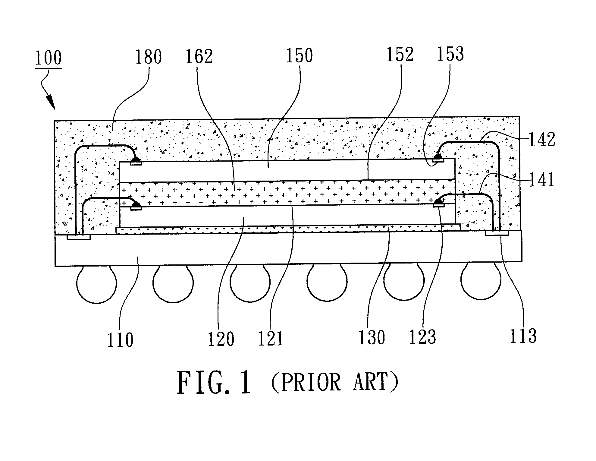
However, when the thickness of FOW adhesive 162 is reduced, the first bonding wires 141 would more easily contact the back surface 152 of the second chip 150 leading to electrical short, especially in packages with long bonding wires.
Moreover, after curing

Method used


Image

  • Multi-chip stacking method to reduce voids between stacked chips
  • Multi-chip stacking method to reduce voids between stacked chips
  • Multi-chip stacking method to reduce voids between stacked chips

Examples


Example

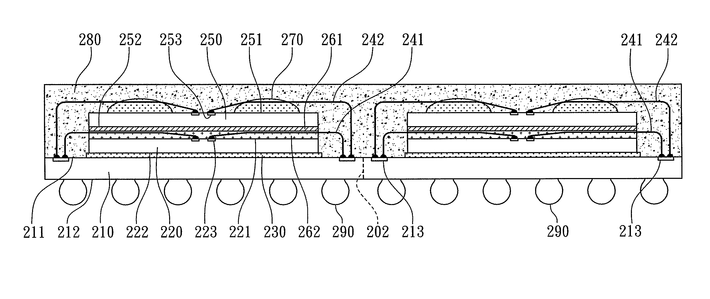
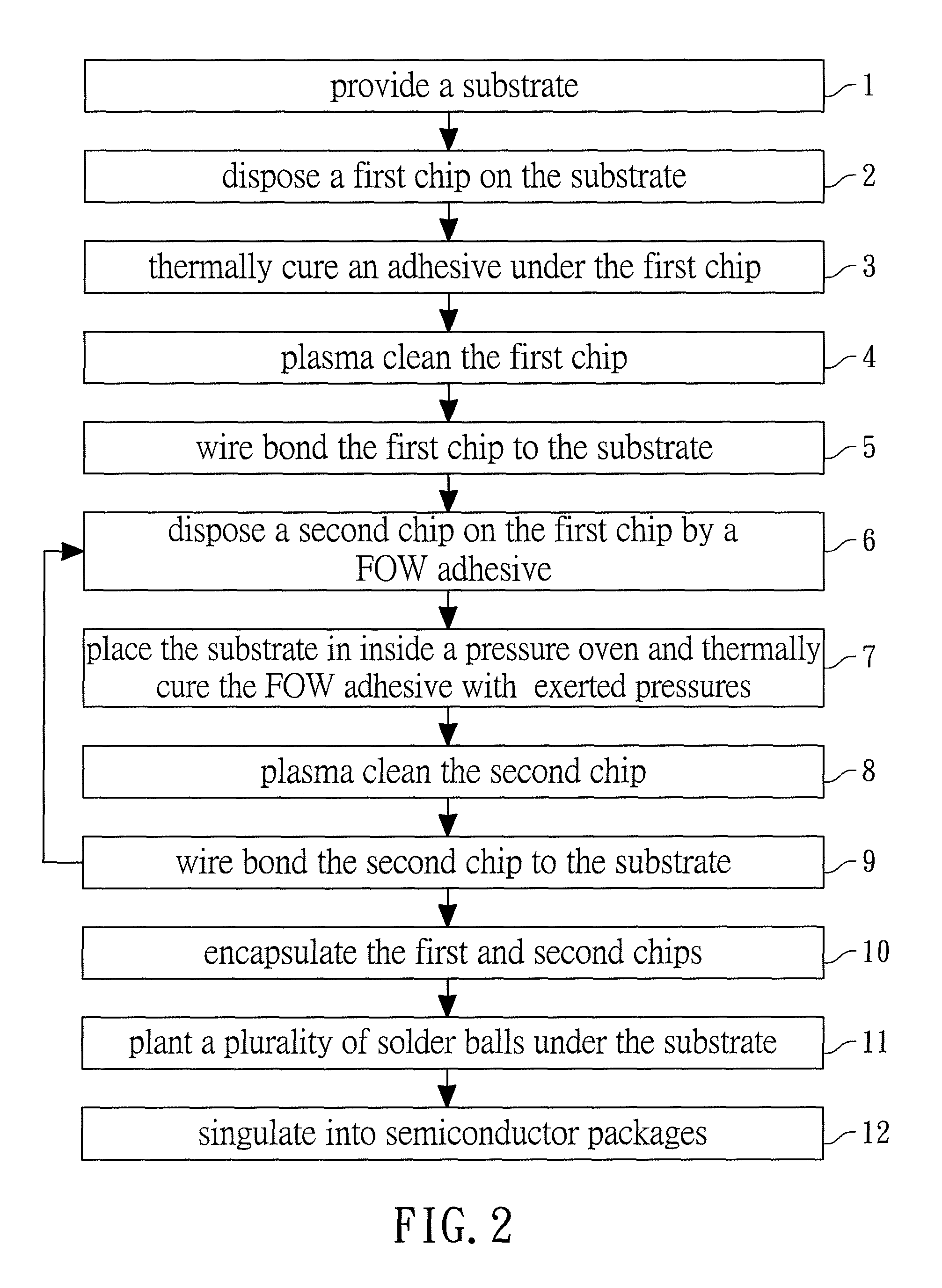
[0021]According to the first embodiment of the present invention, a multi-chip stacking method to reduce voids between stacked chips was illustrated in FIG. 2 for the block diagrams of the process flow and from FIG. 3A to FIG. 3H for the cross-sectional views of each processing step.

[0022]The multi-chip stacking method to reduce voids between stacked chips according to the present invention comprises the following processing steps 1 to 12 as shown in FIG. 2. Therein, step 1 is to provide a substrate 210 as shown in FIG. 3A; step 2 is to dispose a first chip 220 on the substrate 210 as shown in FIG. 3B; step 3 is to thermally cure an adhesive 230 under the first chip 220 referring to FIG. 3B again; step 4 is to plasma clean the first chip 220 referring to FIG. 3B again, step 5 is to wire bond the first chip 220 to the substrate 210 as shown in FIGS. 3C and 4; step 6 is to dispose a second chip 250 on the first chip 220 by a FOW adhesive 262 as shown in FIG. 3D; step 7 is to place the...


PUM


Abstract

A multi-chip stacking method to reduce voids between stacked chips is revealed. A first chip is disposed on a substrate, and a plurality of first bonding wires are formed by wire bonding to electrically connect the first chip and the substrate. A second chip is disposed on an active surface of the first chip where a dielectric layer and a FOW adhesive (film over wire) adhesive are attached onto a back surface of the second chip. The FOW adhesive partially encapsulates the first bonding wires and adheres to the active surface of the first chip. Then, the substrate is placed in a pressure oven to provide a positive pressure greater than one atm during thermally curing the FOW adhesive with exerted pressures. Accordingly, voids can be reduced inside the FOW adhesive during the multi-chip stacked processes where issues of poor adhesion and popcorn between chips can be avoided.

Description

FIELD OF THE INVENTION[0001]The present invention relates to packaging technology of semiconductor devices, more specifically to a multi-chip stacking method to reduce voids between stacked chips with long wire connections.BACKGROUND OF THE INVENTION[0002]In order to meet the requirements of portable electronic devices for minimization and high speed operation with more functions, the development of new technologies has been changed in quarterly bases. Therefore, multi-chip packages have been quite popular to increase the functions or / and the memory capacities within a single package. Chip-on-chip stacked packages have been developed to package two or more chips vertically stacked on each another within a single package to expect a smaller footprint.[0003]As shown in FIG. 1, a conventional multi-chip package (MCP) 100 with chip-on-chip configuration is to vertically stack a plurality of chips 120 and 150 on a substrate 110. Generally speaking, during the packaging processes of the M...

Claims


Application Information

Patent Timeline
IPC IPC(8): H01L21/00
CPCH01L21/561H01L23/3128H01L24/32H01L24/48H01L24/97H01L25/0657H01L25/50H01L21/565H01L24/45H01L2224/32145H01L2224/32225H01L2224/48227H01L2224/48465H01L2224/49171H01L2224/73265H01L2224/97H01L2225/0651H01L2924/01013H01L2924/01029H01L2924/01047H01L2924/01059H01L2924/01079H01L2924/01082H01L2924/014H01L2924/15311H01L2224/45147H01L2224/45144H01L2224/45124H01L2924/01033H01L2924/01006H01L2924/01005H01L24/49H01L2224/85H01L2224/83H01L2224/92247H01L2924/00H01L2924/3512H01L2924/00012H01L2924/00014H01L24/73H01L2224/05554H01L2224/83191H01L2224/85423H01L2224/85447H01L2224/8592H01L2924/181
Inventor LEE, KUO-YUANCHEN, YUNG-HSIANGCHIU, WEN-CHUN
Owner WALTON ADVANCED ENG INC
Why Eureka
Try Eureka