

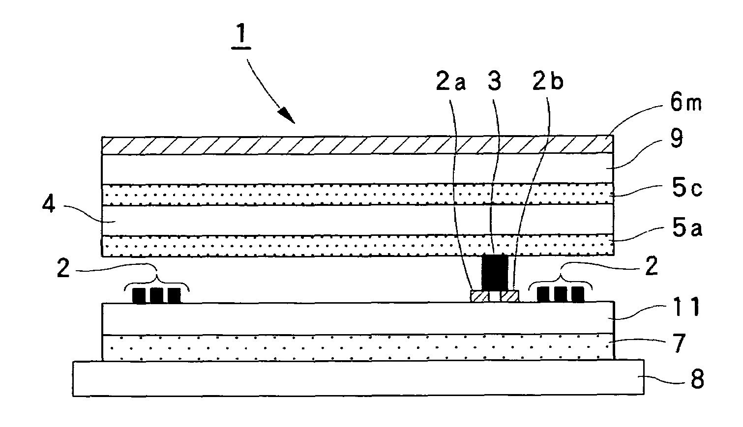
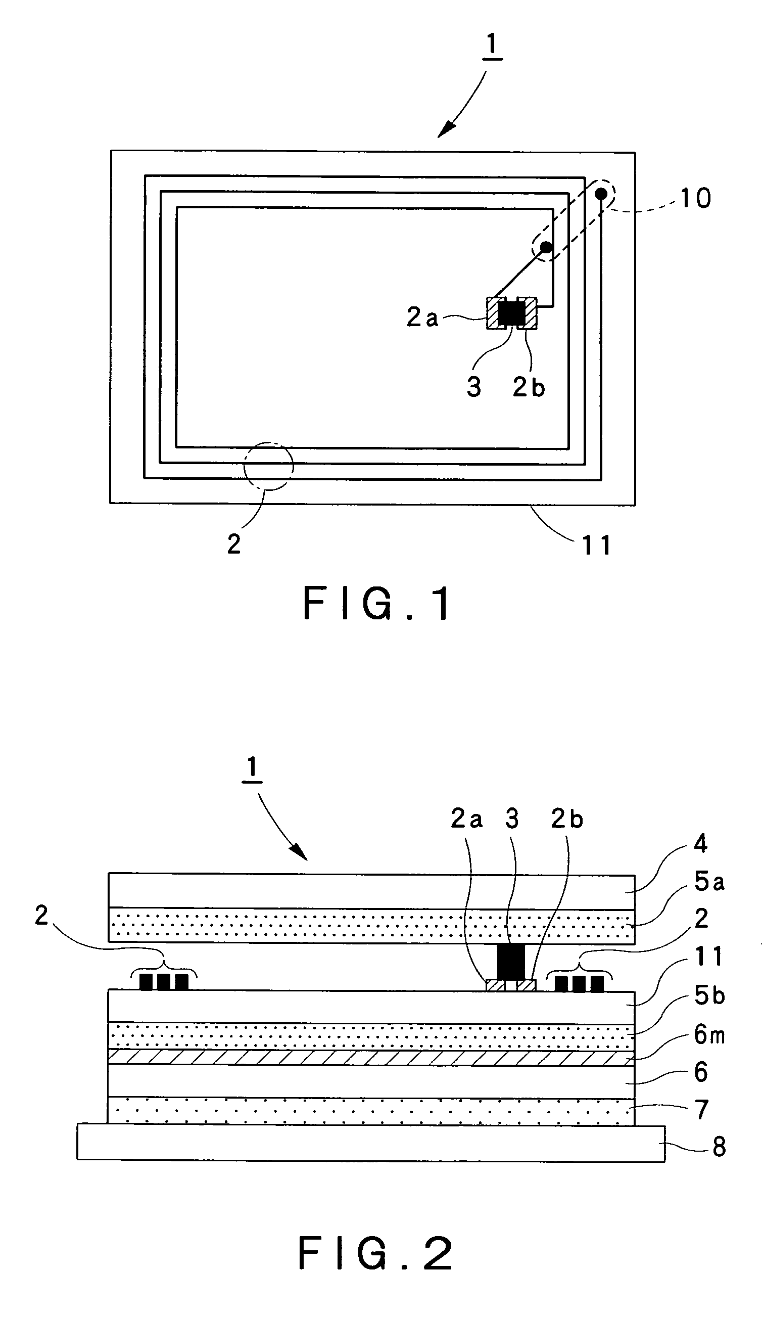
Noncontract IC tag with non-conductive metal film
a non-conductive metal film, non-contact technology, applied in the direction of burglar alarm mechanical actuation, instruments, transportation and packaging, etc., can solve the problems of inability to use practicably, communication failure, and thus reduced magnetic flux for data transmission/reception
- Summary
- Abstract
- Description
- Claims
- Application Information
AI Technical Summary
Benefits of technology
Problems solved by technology
Method used
Image

Examples
example 1
(Preparation of Substrate with Deposited Metal Film)
[0126]A 20-μm thick, biaxially oriented PET film whose surface had been subjected to corona discharge treatment was used as the backing sheet 6. This biaxially oriented PET film was set on a feed roll in a PVD apparatus 20. While feeding the PET film, tin (Sn) was deposited, under the following conditions, on the PET film surface pretreated by corona discharge to form a 20-nm thick film 6m of islands-in-sea structure. In order to evacuate the vacuum deposition chamber 25 to the desired degree of vacuum, argon (Ar) gas was introduced into the vacuum deposition chamber 25.
(Vacuum Deposition Conditions)
[0127]Degree of vacuum: 7.2×10⁻⁴ torr (9.6×10⁻² Pa)
[0128]Cooling drum temperature: 0° C.
[0129]Rate of vacuum deposition: 7 nm / sec
[0130]Metal-depositing surface: surface pretreated by corona discharge
The above cooling drum means the coating drum 24. This applies to the following Examples.
(Production of Noncontact IC Tag)
[0131]A laminate ...
example 2
(Preparation of Substrate with Deposited Metal Film)
[0135]A 12-μm thick, biaxially oriented PET film whose surface had been subjected to corona discharge treatment was used as the surfacing sheet 4. This PET film was set on a feed roll in a PVD apparatus 20. While feeding the PET film, tin (Sn) was deposited, under the following conditions, on the PET film surface pretreated by corona discharge to form a 10-nm thick film 6m of islands-in-sea structure. In order to evacuate the vacuum deposition chamber 25 to the desired degree of vacuum, argon (Ar) gas was introduced into the vacuum deposition chamber 25.
(Vacuum Deposition Conditions)
[0136]Degree of vacuum: 7.4×10⁻⁴ torr (9.9×10⁻² Pa)
[0137]Cooling drum temperature: 0° C.
[0138]Rate of vacuum deposition: 7 nm / sec
[0139]Metal-depositing surface: surface pretreated by corona discharge
(Production of Noncontact IC Tag)
[0140]A complete base film 11 was obtained by forming antenna patterns 2 and connecting an IC chip 3 to both ends of each a...
example 3
(Preparation of Substrate with Deposited Metal Film)
[0143]A 20-μm thick, biaxially oriented PET film whose surface had been subjected to corona discharge treatment was used as the surfacing sheet 4. This PET film was set on a feed roll in a PVD apparatus 20. While feeding the PET film, tin (Sn) was deposited, under the following conditions, on the PET film surface pretreated by corona discharge to form a 10-nm thick film 6m of islands-in-sea structure.
(Vacuum Deposition Conditions)
[0144]Degree of vacuum: 2.6×10⁻⁴ torr (3.5×10⁻² Pa)
[0145]Cooling drum temperature: 0° C.
[0146]Rate of vacuum deposition: 1 nm / sec
[0147]Metal-depositing surface: surface pretreated by corona discharge
(Production of Noncontact IC Tag)
[0148]On the surface of the above-prepared surfacing sheet 4 with the deposited metal film on the side opposite to the deposited metal film, a white-colored concealing layer was formed by gravure printing, using a titanium oxide pigment. In the same manner as in Example 2, this ...
PUM
| Property | Measurement | Unit |
|---|---|---|
| size | aaaaa | aaaaa |
| size | aaaaa | aaaaa |
| height Ra | aaaaa | aaaaa |
Abstract
Description
Claims
Application Information