Eureka AIR delivers breakthrough ideas for toughest innovation challenges, trusted by R&D personnel around the world.

Noncontact IC tag with non-conductive metal film

a non-conductive metal film and ic tag technology, applied in the direction of burglar alarm mechanical actuation, instruments, transportation and packaging, etc., can solve the problems of inability to use practically, reduced magnetic flux for data transmission/reception, and poor communication performance, and achieves moderate luster, excellent communication performance, and the position of the ic tag on the article can be clearly known.

Inactive Publication Date: 2007-06-21
DAI NIPPON PRINTING CO LTD
View PDF5 Cites 14 Cited by
  • Summary
  • Abstract
  • Description
  • Claims
  • Application Information

AI Technical Summary

Benefits of technology

[0033] Preferably, the surface roughness of the non-conductive deposited metal film, determined by atomic force microscopy, is more than 10 nm and 100 nm or less as indicated by the center line average height Ra. This is because a non-conductive deposited metal film having a surface roughness value of 10 nm or less is poor in adhesion to other layer formed on it, while a non-conductive deposited metal film having a surface roughness value of more than 100 nm has no metallic luster and makes the noncontact IC tag less attractive in design.
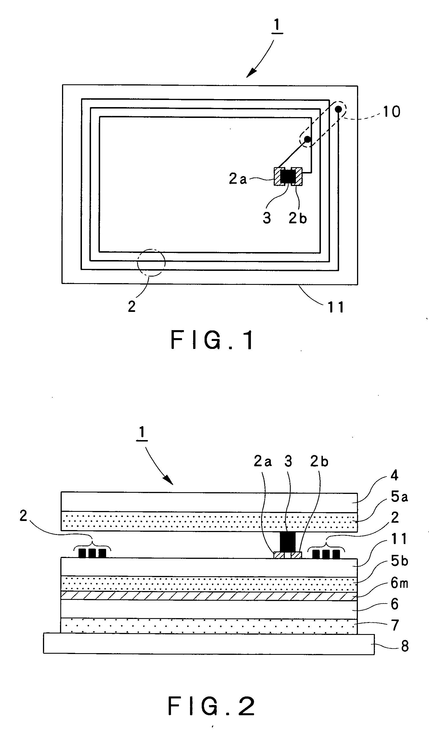
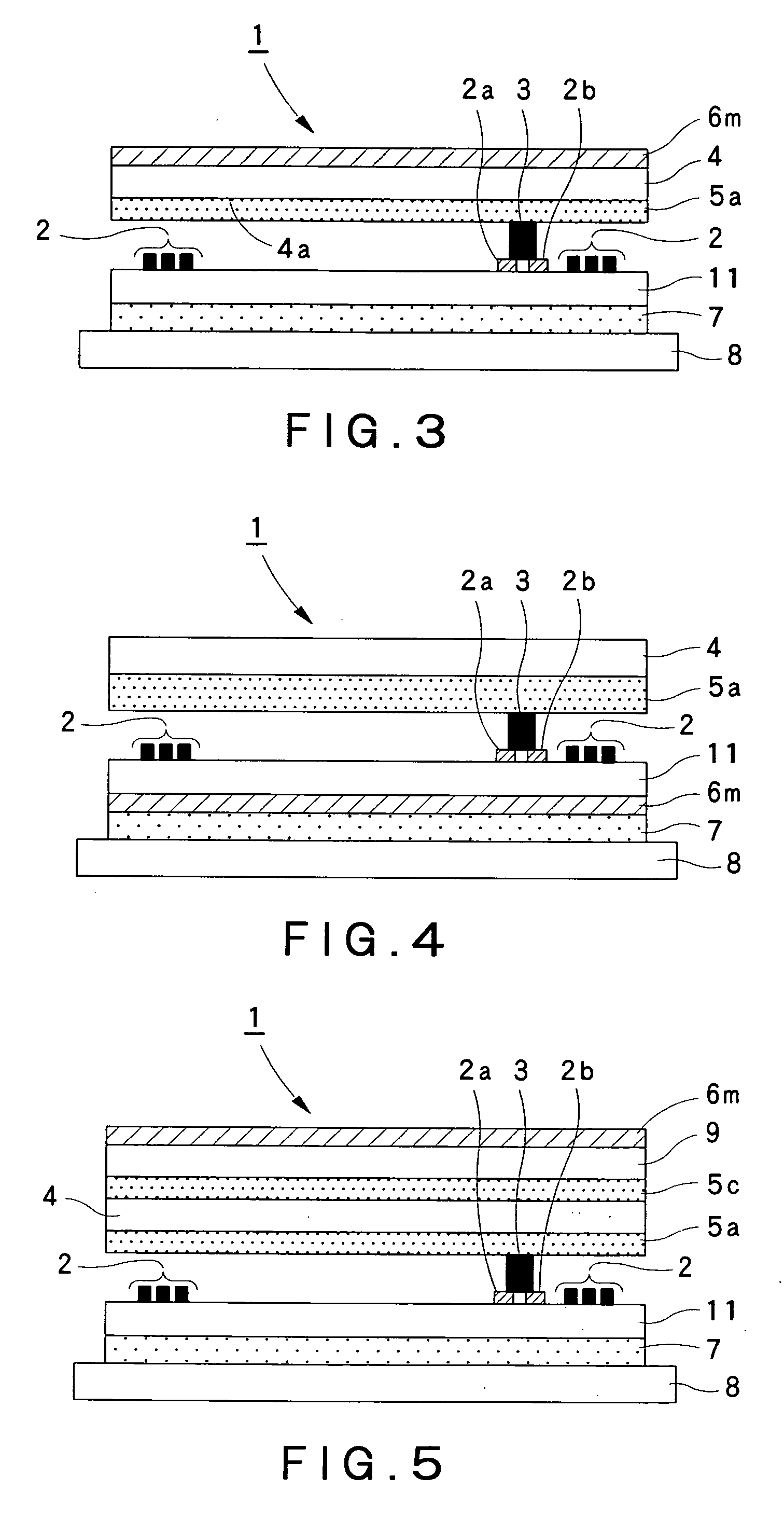
[0042] The noncontact IC tag with a non-conductive metal film has a concealing layer on its inside, and this concealing layer entirely conceals the IC tag circuit to make the noncontact IC tag more attractive in design. Since the IC tag circuit is thus concealed, no users feel uneasy.

Problems solved by technology

In order to meet demand for a decorative noncontact IC tag with a beautiful metallic luster, if a metal material such as aluminum foil or a conventional metallized material is used as the substrate of a noncontact IC tag, the IC tag causes communication failure, so that it cannot be used practically.
A possible cause of the above-described communication failure is as follows: eddy current flows in the metal film owing to the AC magnetic field produced by electromagnetic waves which the noncontact IC tag uses for data transmission / reception; this eddy current produces magnetic flux that repels the magnetic flux for data transmission / reception; the magnetic flux for data transmission / reception is thus reduced, which makes data transmission / reception difficult.
Another possible cause of the above-described communication failure is as follows: an antenna or coil made from an electrically conductive material forms a condenser together with the metal film; the stray capacitance produced by the condenser alters the inductance of the antenna or coil, and the resonance frequency characteristic of the condenser.
However, none of these Patent Documents proposes the use of deposited metal films of islands-in-sea structure for noncontact IC tags.
It is impossible to give a metallic luster to noncontact IC tags by any of the prior art techniques because if a metal is deposited on any constituent layer of a noncontact IC tag, the deposited metal film makes the IC tag poor in communicational performance.

Method used


Image

  • Noncontact IC tag with non-conductive metal film
  • Noncontact IC tag with non-conductive metal film
  • Noncontact IC tag with non-conductive metal film

Examples


example 1

(Preparation of Substrate with Deposited Metal Film)

[0125] A 20-μm thick, biaxially oriented PET film whose surface had been subjected to corona discharge treatment was used as the backing sheet 6. This biaxially oriented PET film was set on a feed roll in a PVD apparatus 20. While feeding the PET film, tin (Sn) was deposited, under the following conditions, on the PET film surface pretreated by corona discharge to form a 20-nm thick film 6m of islands-in-sea structure. In order to evacuate the vacuum deposition chamber 25 to the desired degree of vacuum, argon (Ar) gas was introduced into the vacuum deposition chamber 25.

(Vacuum Deposition Conditions)

[0126] Degree of vacuum: 7.2×10⁻⁴ torr (9.6×10⁻² Pa)

[0127] Cooling drum temperature: 0° C.

[0128] Rate of vacuum deposition: 7 nm / sec

[0129] Metal-depositing surface: surface pretreated by corona discharge

The above cooling drum means the coating drum 24. This applies to the following Examples.

(Production of Noncontact IC Tag)...

example 2

(Preparation of Substrate with Deposited Metal Film)

[0134] A 12-μm thick, biaxially oriented PET film whose surface had been subjected to corona discharge treatment was used as the surfacing sheet 4. This PET film was set on a feed roll in a PVD apparatus 20. While feeding the PET film, tin (Sn) was deposited, under the following conditions, on the PET film surface pretreated by corona discharge to form a 10-nm thick film 6m of islands-in-sea structure. In order to evacuate the vacuum deposition chamber 25 to the desired degree of vacuum, argon (Ar) gas was introduced into the vacuum deposition chamber 25.

(Vacuum Deposition Conditions)

[0135] Degree of vacuum: 7.4×10⁻⁴ torr (9.9×10⁻² Pa)

[0136] Cooling drum temperature: 0° C.

[0137] Rate of vacuum deposition: 7 nm / sec

[0138] Metal-depositing surface: surface pretreated by corona discharge

(Production of Noncontact IC Tag)

[0139] A complete base film 11 was obtained by forming antenna patterns 2 and connecting an IC chip 3 to bo...

example 3

(Preparation of Substrate with Deposited Metal Film)

[0142] A 20-μm thick, biaxially oriented PET film whose surface had been subjected to corona discharge treatment was used as the surfacing sheet 4. This PET film was set on a feed roll in a PVD apparatus 20. While feeding the PET film, tin (Sn) was deposited, under the following conditions, on the PET film surface pretreated by corona discharge to form a 10-nm thick film 6m of islands-in-sea structure.

(Vacuum Deposition Conditions)

[0143] Degree of vacuum: 2.6×10⁻⁴ torr (3.5×10⁻² Pa)

[0144] Cooling drum temperature: 0° C.

[0145] Rate of vacuum deposition: 1 nm / sec

[0146] Metal-depositing surface: surface pretreated by corona discharge

(Production of Noncontact IC Tag)

[0147] On the surface of the above-prepared surfacing sheet 4 with the deposited metal film on the side opposite to the deposited metal film, a white-colored concealing layer was formed by gravure printing, using a titanium oxide pigment. In the same manner as in...


PUM

PropertyMeasurementUnit
Lengthaaaaaaaaaa
Electrical resistanceaaaaaaaaaa
Sizeaaaaaaaaaa

Abstract

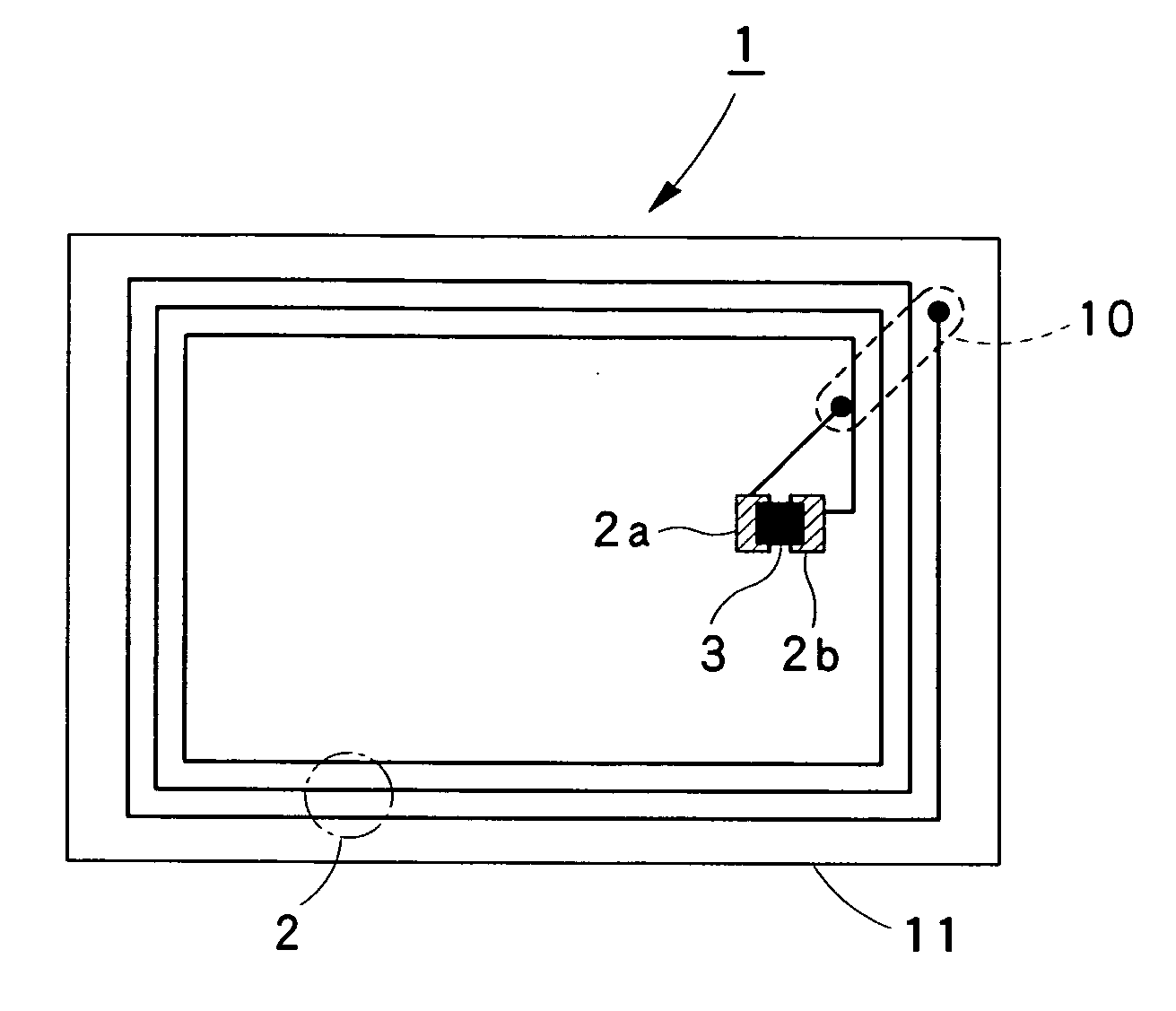
A noncontact IC tag 1 comprises a base film 11, a noncontact IC circuit 2, 3 formed on the base film 11, and a plastic film or paper serving as a surfacing sheet 4, having a non-conductive, lustrous metal film 6m formed by deposition, laminated to the base film 11 on the side of the noncontact IC tag circuit 2, 3. The surface roughness of the non-conductive, lustrous metal film 6m, determined by atomic force microscopy, is more than 10 nm and 100 nm or less as indicated by the center line average height Ra. In the case where the non-conductive, lustrous metal film 6m is formed on the outer surface of the surfacing sheet 4, a concealing layer 4a may further be formed on the inner surface of the surfacing sheet 4 in order to enhance concealing properties.

Description

BACKGROUND OF THE INVENTION [0001] 1. Field of the Invention [0002] The present invention relates to a noncontact IC tag with a non-conductive metal film. More particularly, the present Invention relates to a noncontact IC tag that has a lustrous deposited metal film but is non-conductive, and that is excellent in communication performance. Although the noncontact IC tag with a non-conductive metal film according to the present invention can be used as an ordinary noncontact IC tag, it is particularly favorable for applications where metallic IC tags having decorative properties are desirable. [0003] The technical field of the invention is the production and use of noncontact IC tags. The noncontact IC tags of the present invention are useful mainly in the fields of transportation, distribution, sales control, process control, delivery of commodities, and luggage handling. Specifically, they can be used as tags, labels, slips, tickets, and the like. [0004] 2. Background Art [0005] N...

Claims


Application Information

Patent Timeline
IPC IPC(8): G06K19/06
CPCY10T428/24917G06K19/07749
Inventor ASAKURA, HIROYUKIIMAIZUMI, KIYOSHIIIHARA, TAKESHITAKASAWA, KAZUYUKIKOMADA, MINORU
Owner DAI NIPPON PRINTING CO LTD
Why Eureka
Eureka Blog
Learn More