Wafer test method utilizing conductive interposer

a conductive interposer and test method technology, applied in the field of wafer test methods, can solve the problems of affecting the yield of subsequent chip packaging, notch on or not being favorable for size miniaturization, etc., to achieve the effect of not causing damage to the bond pad, short contact lifetime, and high resistan

Active Publication Date: 2006-06-06
SILICONWARE PRECISION IND CO LTD
View PDF6 Cites 10 Cited by
  • Summary
  • Abstract
  • Description
  • Claims
  • Application Information

AI Technical Summary

Benefits of technology

[0013]Therefore, the wafer test method according to the invention is carried out for a fabricated wafer prior to forming bumps on the wafer, using a conductive interposer having one side with test pads and the other side with test bumps electrically connected to the test pads. The conductive interposer is mounted on the wafer comprising a plurality of chips, wherein the test bumps are in electrical contact with bond pads formed on active surfaces of the chips. Then, test probes are used to contact the test pads to perform tests for the chips. This wafer test method is beneficially performed prior to forming bumps on the wafer, such that the prior-art drawback of damaging bumps on the wafer by contacting test probes with the bumps on the wafer can be eliminated, and the conductive interposer mounted on the wafer prevents the test probes from physical contact with the bond pads on the chips, thereby not causing damage to the bond pads. Moreover, compared to the prior art using test probes to directly contact bond pads on the wafer, the use of the conductive interposer according to the invention allows moderate contact and increase in contact area between the conductive interposer and the bond pads on the wafer, such that the wafer tests can be more accurately and precisely performed. In addition, compared to using an expensive anisotropic conductive film (ACF) having high resistance and short contact lifetime, the conductive interposer according to the invention is more cost-effectively fabricated and can be used repeatedly, thereby reducing the overall fabrication costs.

Problems solved by technology

However, this test method undesirably causes a notch on or damage to the bond pads 13 (FIG. 6A) or the UBM structure 15 by direct contact of the test probes 2.
However, this method easily damages the bumps 14 and thus affects yield of subsequent chip packaging.
However, this bond-pad arrangement requires additional surface area on the wafer for disposing the test bond pads, thereby not favorable for size miniaturization.
However, this technology is defective that the ACF has high conductive resistance and is only suitable for mediating the current but not for test performance; further, the ACF has short contact lifetime (about 50 times) and cannot be used repeatedly, and the ACF is expensively fabricated, thereby undesirably increasing the fabrication costs.
Therefore, the problem to be solved herein is to provide a wafer test method carried out before forming bumps on the wafer, which would not damage bond pads on the wafer and not increase fabrication costs.

Method used


Image

  • Wafer test method utilizing conductive interposer
  • Wafer test method utilizing conductive interposer
  • Wafer test method utilizing conductive interposer

Examples


Embodiment Construction

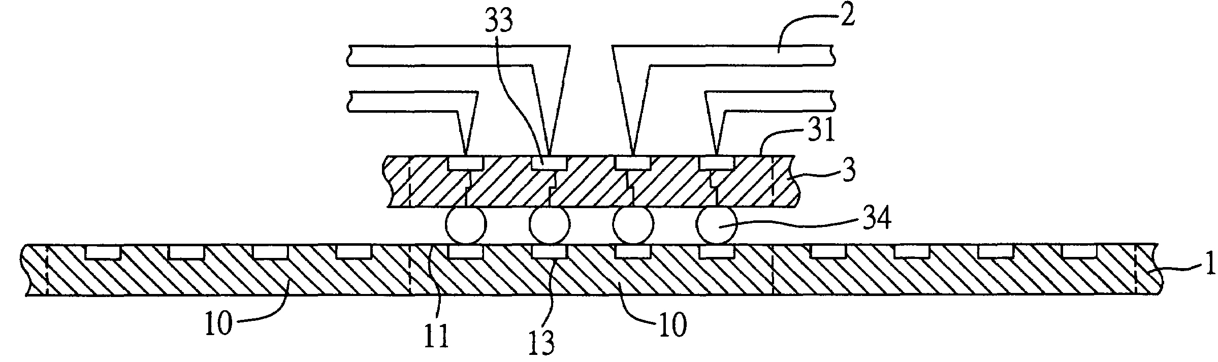
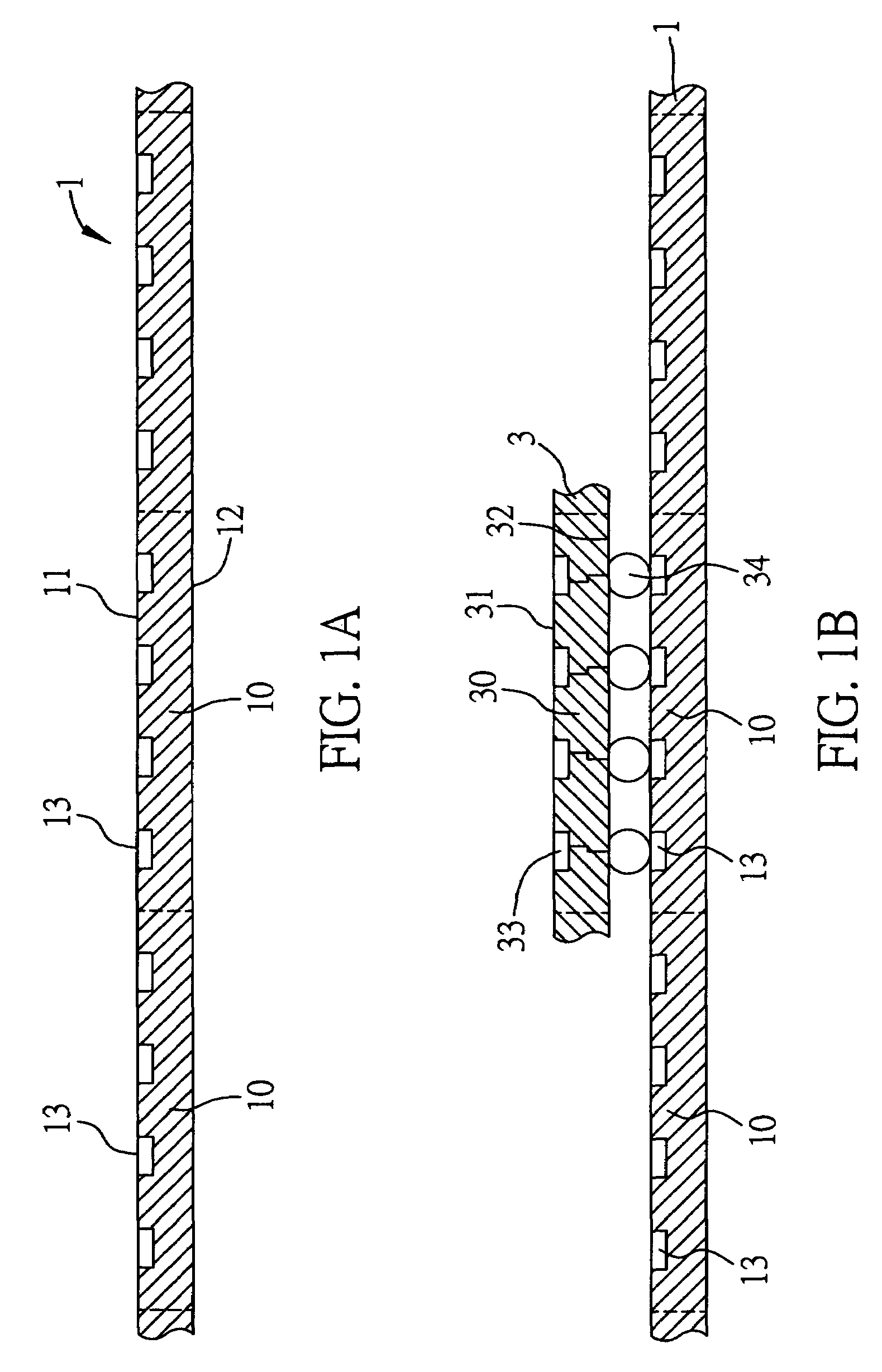
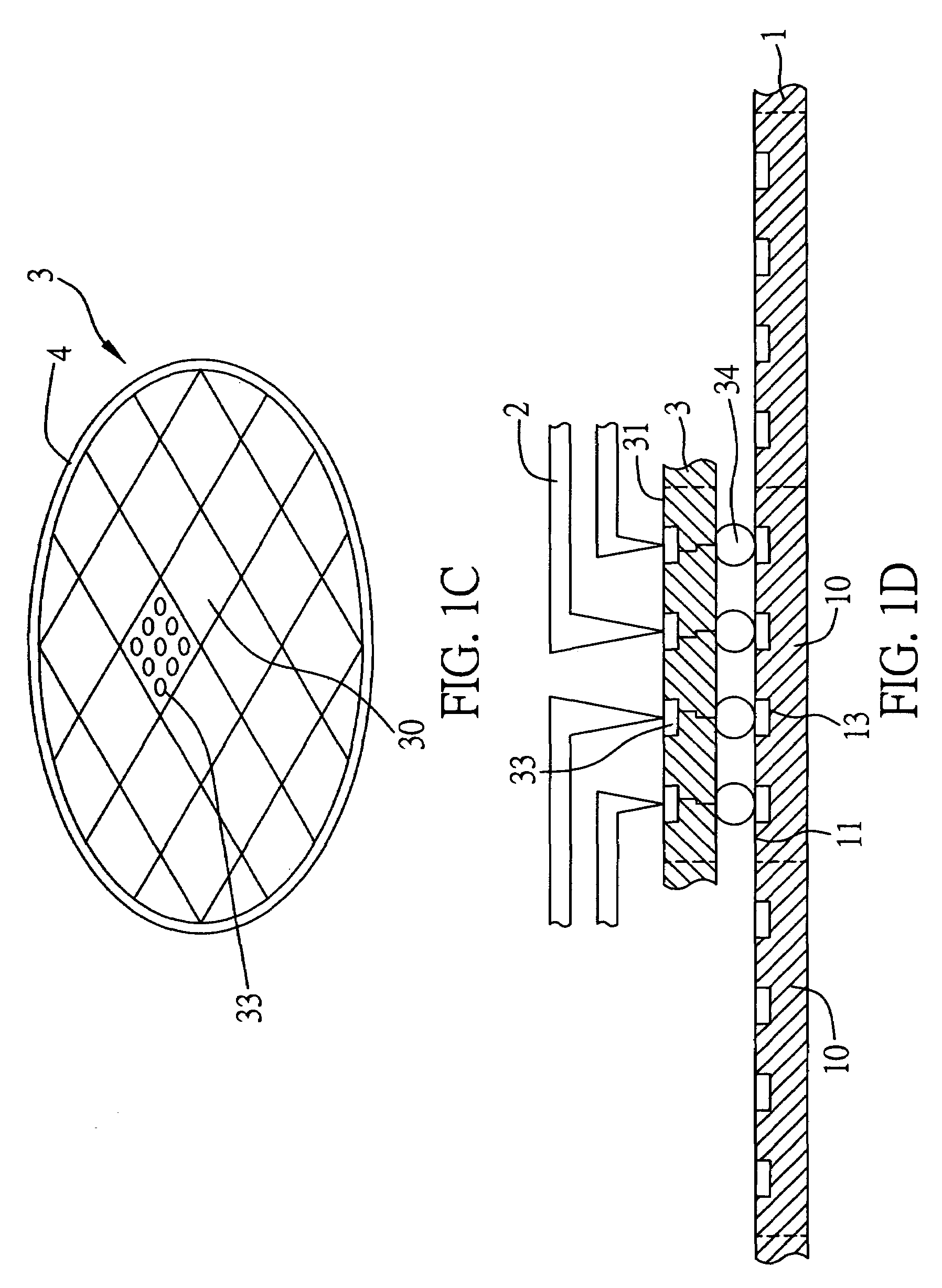
[0021]As shown in FIG. 1A, a wafer test method proposed by the present invention is first to prepare a wafer 1 integrally formed of a plurality of chips 10, wherein each of the chips 10 has an active surface 11 and an opposite inactive surface 12, and a plurality of bond pads 13 are formed on the active surface 11 of each chip 10. The wafer 1 is fabricated by conventional technology, thereby not further detailed herein.

[0022]Referring to FIG. 1B, the next step is to mount a conductive interposer 3 on the wafer 1 and electrically connect the conductive interposer 3 to the chips 10. The conductive interposer 3 has a first surface 31 and an opposite second surface 32, wherein the first surface 31 is formed with a plurality of test pads 33 thereon, and the second surface 32 is formed with a plurality of test bumps 34 electrically connected to the test pads 33, the test bumps 34 corresponding to the bond pads 13 of the chips 10 (one is shown), such that the test bumps 34 are in electrica...


PUM


Abstract

A wafer test method is performed for a wafer prior to forming bumps on the wafer, using a conductive interposer having one side with test pads and the other side with test bumps electrically connected to the test pads. The conductive interposer is mounted on the wafer having a plurality of chips, wherein the test bumps are in electrical contact with bond pads on active surfaces of the chips. Test probes are used to contact the test pads to perform tests for the chips. This wafer test method is beneficially performed prior to forming bumps on the wafer, such that the prior-art drawback of damaging bumps on the wafer by contacting test probes with the bumps on the wafer can be eliminated, and the conductive interposer mounted on the wafer prevents the test probes from physical contact with the bond pads on the chips, thereby not damaging the bond pads.

Description

FIELD OF THE INVENTION[0001]The present invention relates to wafer test methods, and more particularly, to a method for testing a wafer performed prior to forming bumps on the wafer.BACKGROUND OF THE INVENTION[0002]Semiconductor package is a resin-encapsulated structure incorporated with at least one integrated circuit component such as semiconductor chip that is enclosed by an encapsulating resin for protection. A chip carrier (e.g. substrate, lead frame, etc.) is usually employed to mount and electrically connect the semiconductor chip. A conventional electrical connection is achieved by using a plurality of conductive bonding wires (such as gold wires) to interconnect an active surface of the chip and the chip carrier, and the bonding wires are also encapsulated by the encapsulating resin. However, the bonding wires possess predetermined length and loop height, such that they occupy a certain extent of surface area on the chip carrier; further, an encapsulation body formed by the...

Claims


Application Information

Patent Timeline
Patent Type & Authority Patents(United States)
IPC IPC(8): G01R31/02G01R31/28
CPCG01R31/2831
Inventor PU, HAN-PING
Owner SILICONWARE PRECISION IND CO LTD
Why Eureka
Try Eureka