Nitride semiconductor light emitting device array

a light-emitting device and semiconductor technology, applied in the direction of semiconductor devices, basic electric elements, electrical appliances, etc., can solve the problems of many crystal defects in the nitride crystal, and achieve the effect of maximizing the light-emitting area

Inactive Publication Date: 2013-11-19
SAMSUNG ELECTRONICS CO LTD
View PDF25 Cites 5 Cited by
  • Summary
  • Abstract
  • Description
  • Claims
  • Application Information

AI Technical Summary

Benefits of technology

The present invention provides a nitride semiconductor light emitting device array with improved arrangement of hexagonal pyramid light emission structures and windows to maximize the light emission area. Additionally, a vertical-structure nitride semiconductor light emitting device array includes a light-transmitting conductive layer, a reflective electrode layer, and a conductive support structure to further improve the light extraction efficiency. The "technical effects" of the invention include increased light emission area and improved light extraction efficiency.

Problems solved by technology

Without a suitably compatible substrate, however, nitride crystals tend to have many crystal defects.

Method used


Image

  • Nitride semiconductor light emitting device array
  • Nitride semiconductor light emitting device array
  • Nitride semiconductor light emitting device array

Examples


Embodiment Construction

[0029]Exemplary embodiments of the present invention will now be described in detail with reference to the accompanying drawings.

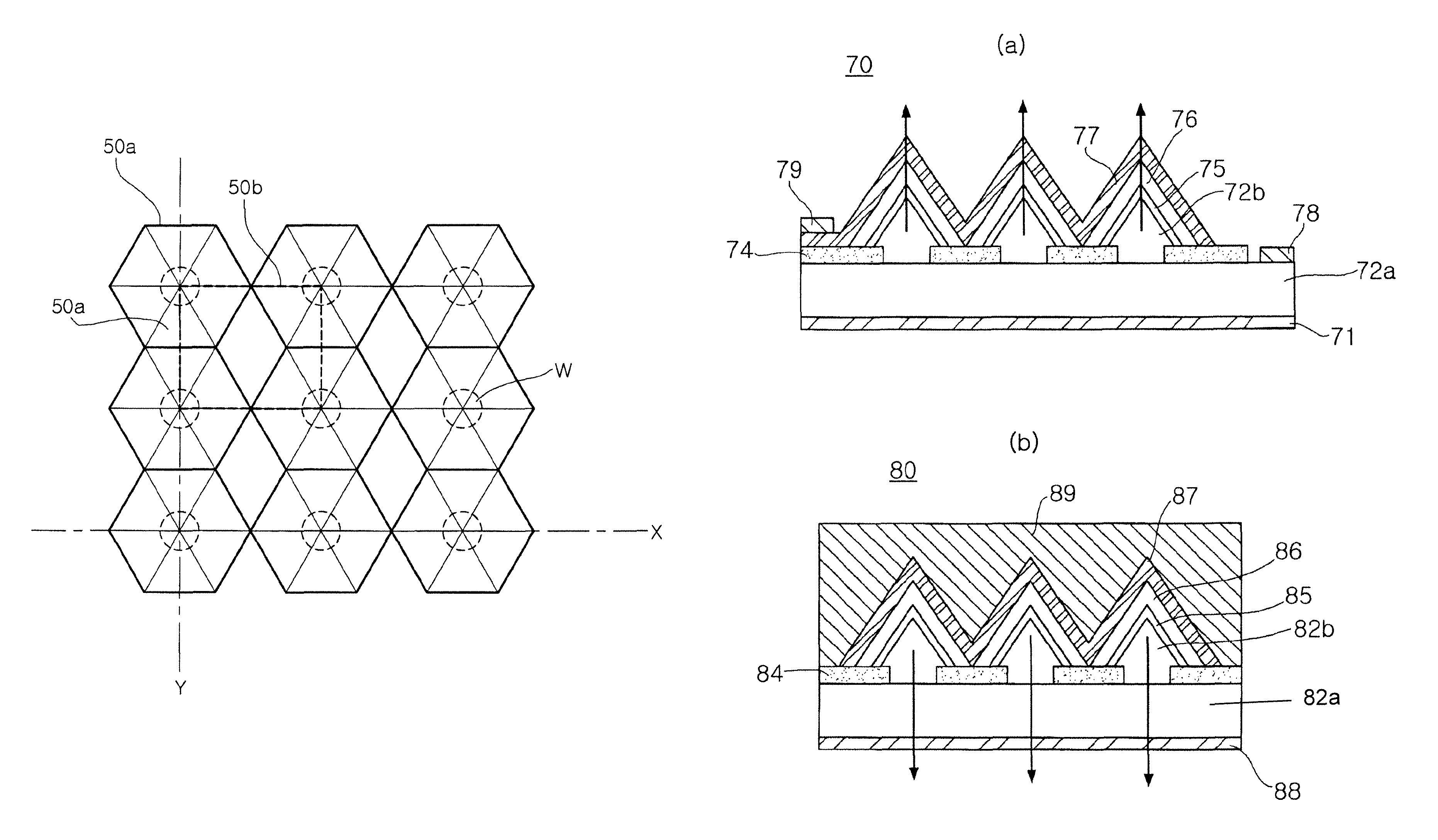
[0030]FIG. 3 is a schematic plan view illustrating a hexagonal pyramid nitride light emitting device array according to an embodiment of the present invention.

[0031]FIG. 3 illustrates a light emitting device array with hexagonal pyramid nitride light emission structures 30 grown on a dielectric layer 34 with a plurality of windows W formed therethrough. As described herein with reference to FIG. 1, each of the hexagonal pyramid nitride light emission structure 30 may be understood as including a first conductivity upper nitride semiconductor layer, an active layer and a second conductivity nitride semiconductor layer selectively grown in the window W.

[0032]For an optimal arrangement of the hexagonal pyramid nitride light emission structures 30 according to the present invention, the plurality of windows W are disposed in an equilateral triangular arrangeme...


PUM


Abstract

A nitride semiconductor light emitting device array, which includes a dielectric layer formed on a first conductivity lower nitride semiconductor layer, having a plurality of windows. Each of a plurality of hexagonal pyramid light emission structures is grown from a surface of the first conductivity lower nitride semiconductor layer exposed through each of the windows and onto a peripheral area of the window of the dielectric layer. Each of the hexagonal pyramid light emission structures includes a first conductivity upper nitride semiconductor layer, an active layer and a second conductivity nitride semiconductor layer formed in their order. The windows are disposed in such a triangular arrangement that side surfaces of the adjacent hexagonal pyramid light emission structures face each other. Also, a distance between bases of the adjacent hexagonal pyramid light emission structures is less than 0.3 times an interval between centers of the windows of the adjacent hexagonal pyramid light emission structures.

Description

CROSS-REFERENCE TO RELATED APPLICATIONS[0001]This application is a Divisional of U.S. application Ser. No. 11 / 819,785, filed on Jun. 29, 2007, now abandoned which claims the benefit of Korean Patent Application No. 2006-0060699 filed on Jun. 30, 2006, in the Korean Intellectual Property Office, the disclosures of which are incorporated herein by reference.BACKGROUND OF THE INVENTION[0002]1. Field of the Invention[0003]The present invention relates to a light emitting device array and, more particularly, to a light emitting device array having a plurality of hexagonal pyramid light emitting structures formed by selective growth.[0004]2. Description of the Related Art[0005]Recently, researches have been actively conducted on semiconductor light emitting devices as a new light source that can replace filament-based light bulbs and fluorescent lamps. In particular, the researches on light emitting diodes (LEDs) using nitride compound semiconductors such as GaN have been gaining attentio...

Claims


Application Information

Patent Timeline
Patent Type & Authority Patents(United States)
IPC IPC(8): H01L33/20H01L33/08H01L33/32H01L33/42
CPCH01L33/24
Inventor YOON, SANG HOMIN, KYEONG IK
Owner SAMSUNG ELECTRONICS CO LTD
Why Eureka
Try Eureka