A kind of oled device comprising patterned transmission layer and its preparation method
A transmission layer and patterning technology, applied in semiconductor/solid-state device manufacturing, electric solid-state devices, semiconductor devices, etc., can solve the problems of loss of effective light-emitting area, special preparation process, complex structure, etc., and achieve the effect of improving light output efficiency
- Summary
- Abstract
- Description
- Claims
- Application Information
AI Technical Summary
Problems solved by technology
Method used
Image
Examples
Embodiment 1
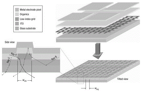
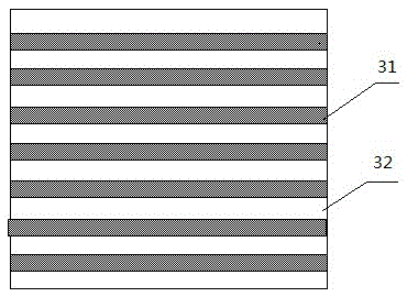
[0062] This embodiment provides a patterned transmission layer, the patterned transmission layer includes a conductive high-refractive-index region and a conductive low-refractive-index region, and the difference in refractive index between the high-refractive-index region and the low-refractive-index region is Value > 0.2. As a preferred implementation manner, the difference in refractive index between the high refraction region and the low refraction region can be selected to be >0.3. As a possible implementation manner, the refractive index of the high refractive index region is between 1.8-3.0; the refractive index of the low refractive index region is between 1.6-2.3.
[0063] In this embodiment, the high refractive index region is made of high refractive index material NPB with a refractive index of 1.8; the low refractive index region is made of NPB with a refractive index of 1.8 and MgF with a refractive index of 1.3. 2 Prepared by mixing, wherein NPB with a refractiv...
Embodiment 2
[0069] The OLED device in this embodiment has the same structure as the OLED device in Embodiment 1;
[0070] The preparation method is also the same, except that when preparing the patterned transmission layer, the low refractive index region uses NPB with a refractive index of 1.8 and MgF with a refractive index of 1.3. 2 Prepared by mixing, wherein NPB with a refractive index of 1.8 accounts for 70 parts by weight, and MgF with a refractive index of 1.3 2 Accounting for 30 parts by weight.
Embodiment 3
[0072] The OLED device in this embodiment has the same structure as the OLED device in Embodiment 1;
[0073] The preparation method is also the same, except that when preparing the patterned transmission layer, the low refractive index region uses NPB with a refractive index of 1.8 and MgF with a refractive index of 1.3. 2 Prepared by mixing, wherein NPB with a refractive index of 1.8 accounts for 50 parts by weight, and MgF with a refractive index of 1.3 2 Accounting for 50 parts by weight.
PUM
 Abstract
Description
Claims
Application Information


