Electromagnetic-wave-absorbing film and electromagnetic wave absorber comprising it

a technology of electromagnetic waves and film, which is applied in the field of electromagnetic wave absorber and film comprising electromagnetic waves, can solve the problems of not being able to absorb electromagnetic waves in a wide frequency range without, being difficult to be disposed in the apparatus casing, and being heavy and bulky, and achieve excellent electromagnetic wave absorbability

Inactive Publication Date: 2013-12-03
KAGAWA SEIJI
View PDF18 Cites 13 Cited by
  • Summary
  • Abstract
  • Description
  • Claims
  • Application Information

AI Technical Summary

Benefits of technology

[0004]Accordingly, an object of the present invention is to provide an inexpensive, electromagnetic-wave-absorbing film having excellent electromagnetic wave absorbability in a wide frequency range, and an electromagnetic wave absorber comprising it.DISCLOSURE OF THE INVENTION
[0011]The electromagnetic wave absorber according to a further preferred embodiment of the present invention comprises a pair of outermost, flat, electromagnetic-wave-absorbing film, and at least one corrugated electromagnetic-wave-absorbing film sandwiched by the flat electromagnetic-wave-absorbing films, adjacent electromagnetic-wave-absorbing films being arranged such that their linear scratches are substantially perpendicular to each other, and that their contact areas are bonded to each other, thereby having reduced anisotropy of electromagnetic wave absorbability and self-supportability.

Problems solved by technology

Shields widely used at present are metal sheets or nets, etc., but they are heavy and bulky, and not easy to be disposed in apparatus casings.
However, the linear patterns and the network patterns illustrated in this reference are all periodic, absorbing only electromagnetic waves in particular frequencies, but failing to absorb electromagnetic waves in a wide frequency range without leak.
In addition, because the patterns are obtained by etching, this electromagnetic-wave-absorbing shield is inevitably expensive.
However, this electromagnetic wave shield does not have linear gaps in the vapor-deposited layer, exhibiting low electromagnetic wave absorbability.

Method used


Image

  • Electromagnetic-wave-absorbing film and electromagnetic wave absorber comprising it
  • Electromagnetic-wave-absorbing film and electromagnetic wave absorber comprising it
  • Electromagnetic-wave-absorbing film and electromagnetic wave absorber comprising it

Examples


example 1

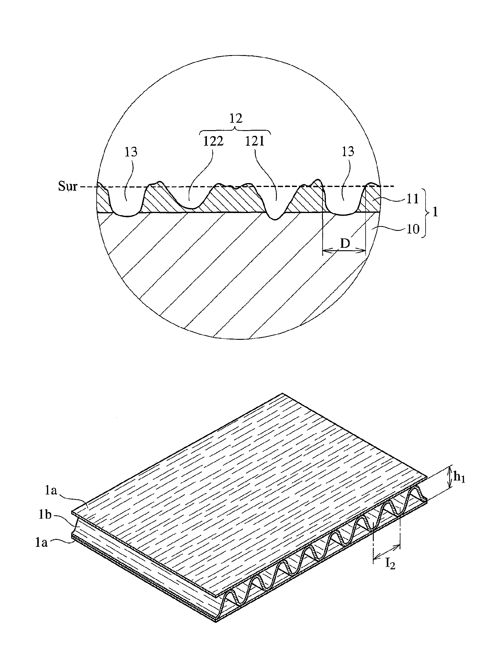
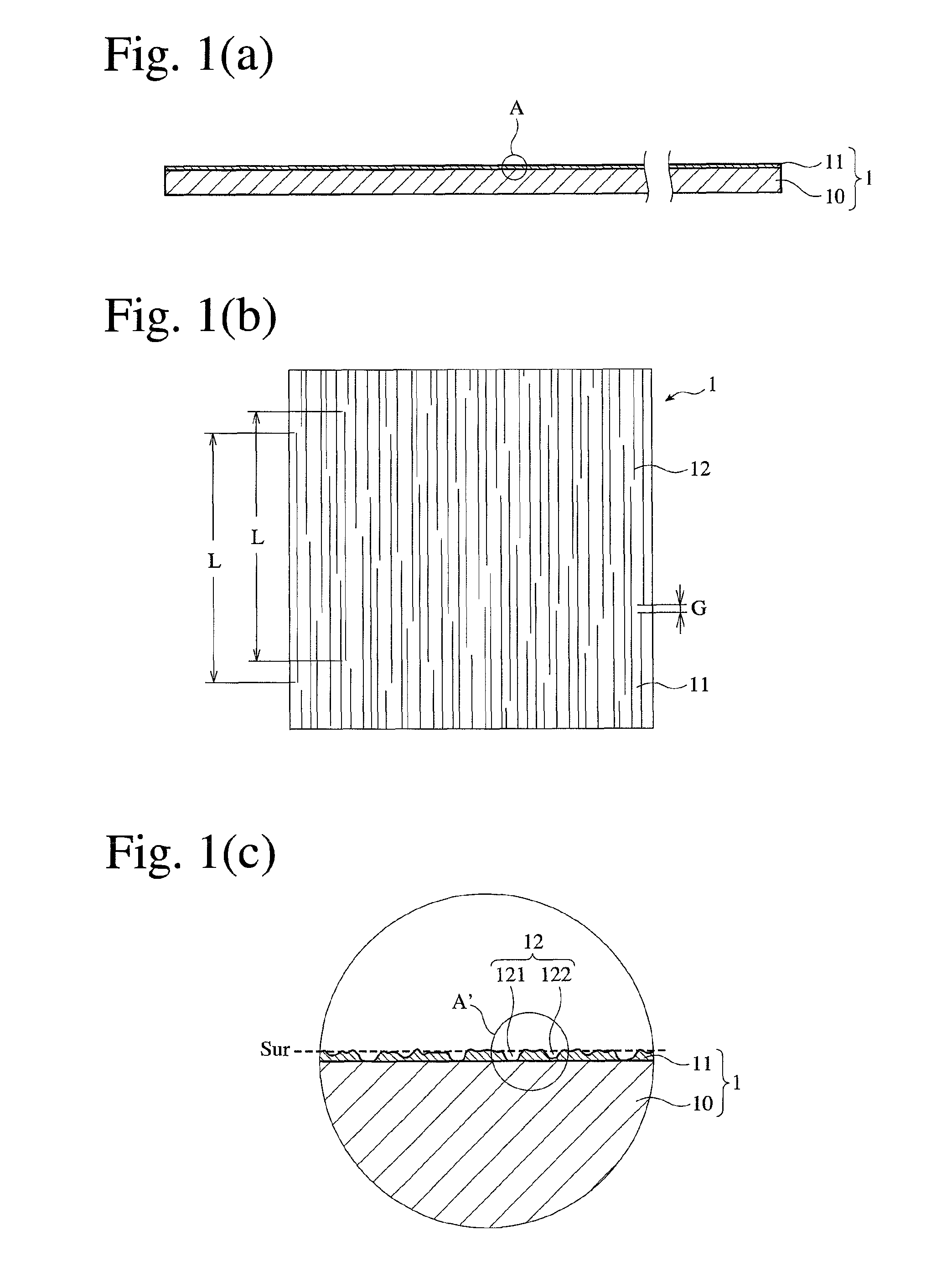
[0091]A 0.05-μm-thick aluminum layer was formed on a surface of a biaxially oriented polyethylene terephthalate (PET) film [thickness: 12 μm, dielectric constant: 3.2 (1 MHz), dissipation factor: 1.0% (1 MHz), melting point: 265° C., and glass transition temperature: 75° C.] by a vacuum deposition method, to produce a composite film. Using the apparatus shown in FIGS. 5(a) and 5(b), a roll 2 having electroplated fine diamond particles having a particle size distribution of 50-80 μm was brought into sliding contact with the aluminum layer of the composite film 1′ under the following conditions.[0092]Moving speed of composite film 1′: 10 in / minute,[0093]Peripheral speed of roll 2: 350 m / minute,[0094]Tension of composite film 1′: 0.1 kgf / cm width, and[0095]Winding angle θ of film: 30°.

[0096]Optical photomicrographical observation revealed that the resultant electromagnetic-wave-absorbing film had the following linear scratches:[0097]Range of widths W: 0.5-5 μm,[0098]Average width Wav: ...

example 2

[0104]The same electromagnetic-wave-absorbing film as in Example 1 except for having fine pores was produced. The fine pores had an average opening diameter of 3 μm, and an average density of 5×10⁴ / cm2. The surface resistance of this electromagnetic-wave-absorbing film was 900 Ω / square and 15 Ω / square, respectively, in directions perpendicular and parallel to the linear scratches. The electromagnetic wave absorbability measured in the same manner as in Example 1 is shown in FIG. 18.

example 3

[0105]An electromagnetic wave absorber was obtained by disposing the electromagnetic-wave-absorbing films of Examples 1 and 2 in parallel with a gap of 5.0 mm such that their linear scratches were substantially perpendicular to each other, and arranged between the antennas 50, 60 with the electromagnetic-wave-absorbing film of Example 1 on the side of the antenna 50, to evaluate the electromagnetic wave absorbability in the same manner as in Example 1. The results are shown in FIG. 19.


PUM

PropertyMeasurementUnit
widthaaaaaaaaaa
widthaaaaaaaaaa
widthaaaaaaaaaa

Abstract

An electromagnetic-wave-absorbing film comprising a plastic film, and a single- or multi-layer, thin metal film formed on at least one surface of the plastic film, the thin metal film being provided with large numbers of substantially parallel, intermittent, linear scratches with irregular widths and intervals.

Description

FIELD OF THE INVENTION[0001]The present invention relates to an inexpensive, electromagnetic-wave-absorbing film having excellent electromagnetic wave absorbability in a wide frequency range, and an electromagnetic wave absorber comprising it.BACKGROUND OF THE INVENTION[0002]Shields for preventing the leak and intrusion of electromagnetic waves are used in electronic and communications apparatuses such as cell phones, personal computers, etc. Shields widely used at present are metal sheets or nets, etc., but they are heavy and bulky, and not easy to be disposed in apparatus casings. As a light-weight, electromagnetic-wave-absorbing shield, which can be easily disposed in plastic casings, etc., JP 9-148782 A proposes a shield comprises a first aluminum film vapor-deposited on one surface of a plastic film and etched to have a non-conductive linear pattern, and a second aluminum film vapor-deposited on the other surface of the plastic film and etched to have a network pattern. However...

Claims


Application Information

Patent Timeline
Patent Type & Authority Patents(United States)
IPC IPC(8): H05K9/00
CPCB32B3/30B32B15/08H05K9/0086H05K9/0056E04B2001/925Y10T428/2457Y10T428/24322Y10T428/24149B32B3/12B32B3/28B32B15/20B32B27/281B32B27/285B32B27/286B32B27/302B32B27/308B32B27/32B32B27/34B32B27/36B32B27/365B32B2307/102B32B2307/202B32B2307/212B32B2307/304B32B2307/50B32B2307/546B32B2307/714B32B2419/00B32B2457/00H05K9/0088
Inventor KAGAWA, SEIJI
Owner KAGAWA SEIJI
Why Eureka
Try Eureka