

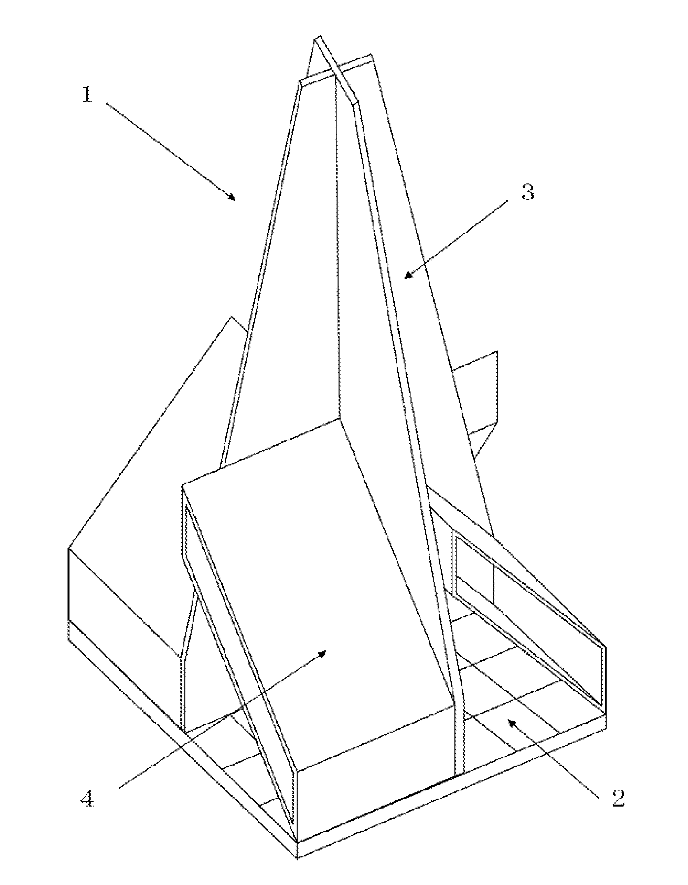
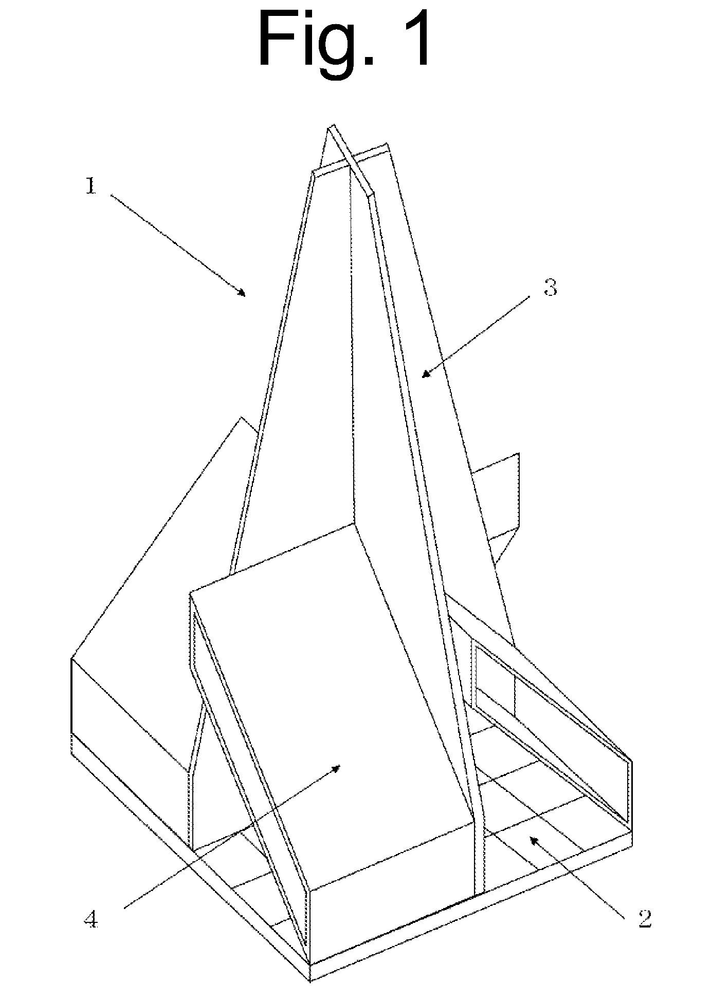
Combined electromagnetic wave absorber
a combined electromagnetic and absorber technology, applied in the field of electromagnetic absorbers, can solve the problems of inability to install, inhibit the arrival of electromagnetic waves at the magnetic absorber plate, and the weight and volume of conventional solid electromagnetic wave absorbers, so as to improve the effective absorption of electromagnetic waves, improve the and excellent electromagnetic wave absorption property
- Summary
- Abstract
- Description
- Claims
- Application Information
AI Technical Summary
Benefits of technology
Problems solved by technology
Method used
Image

Examples
example 1
[0038]Carbon fiber of 3 mm in fiber length and 7 μm in fiber diameter was dispersed into pulp so that its carbon content was 1 mass %, and used for paper making. In this manner, an electrically conductive sheet was manufactured. This electrically conductive sheet was affixed to the front and back of an electrically nonconductive paper sheet with the paper sheet as the inner core, thereby making a corrugated cardboard sheet of a thickness of 3 mm. The sheet was then cut into pieces of 300 mm (width)×1530 mm (length). Note that the carbon content with respect to the total mass of the corrugated cardboard sheet was 0.4 mass %. The resulting corrugated cardboard sheet was dimensioned in accordance with the developed view shown in FIG. 5, so that side “a” was 600 mm, “b” was 150 mm, and “d” was 30 mm, and then bent. An adhesive was then applied to the overlap portion (d) for assembly, thereby forming a 2-layer electromagnetic wave absorber structure with a space layer (a low dielectric l...
example 2
[0039]The corrugated cardboard sheet similar to that of Example 1 was used to complete a compact electromagnetic wave absorber. Here, the compact electromagnetic wave absorber was similar to that of Example 1 except that the “b” of the developed view shown in FIG. 5 was 100 mm and the space layer (low dielectric layer) was 100 mm.
example 3
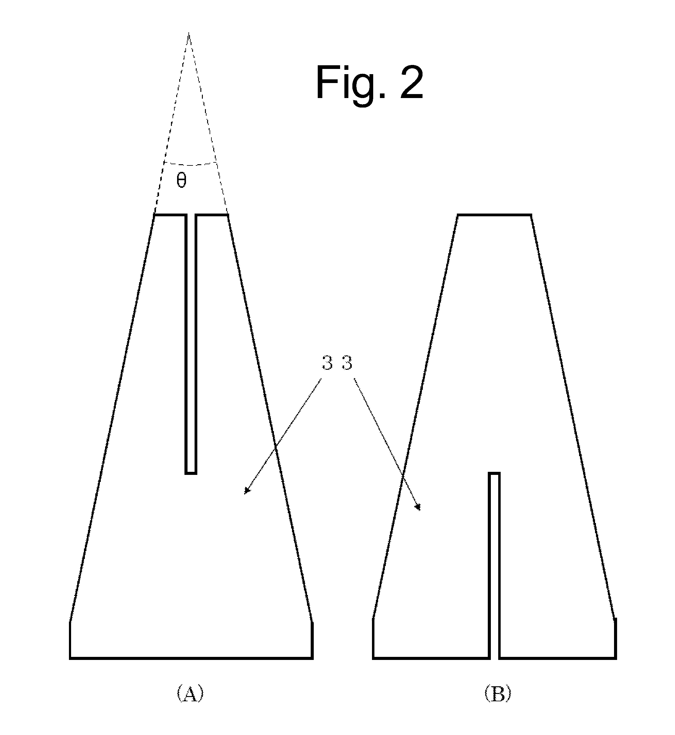
[0040]The corrugated cardboard sheet similar to that of Example 1 was used to make a plurality of hollow quadrangular pyramids based on the developed view shown in FIG. 7(A). Here, the length of the bottom side of the pyramid “e” was 150 mm and its height “f” was 500 mm. Furthermore, based on the developed view shown in FIG. 7(B), a plurality of regular square tubes were made which had a bottom side “e” of 150 mm and a height “g” of 100 mm. As shown in FIG. 7(D), the two pyramids and one regular square tube were used to make a 2-layered electromagnetic wave absorber, in which the bottom side of one pyramid and the bottom side of the other pyramid were aligned with the upper side and the lower side of the regular square tube, respectively, to form a space layer (a low dielectric layer) of 100 mm therein. The electromagnetic wave absorbers formed in this manner were disposed in the four spaces defined by the crossed electromagnetic wave absorber, four at each space, 16 in total, thus ...
PUM
 Abstract
Description
Claims
Application Information