Electrical connector having an electronic device

a technology of electronic devices and electrical connectors, which is applied in the direction of coupling device connections, capacitors, electrical apparatus, etc., can solve the problems of voids formed in solder, higher melting point of solder, and difficult melting, so as to reduce the cross-sectional area a, increase the heat q moving in an object, and reduce the thickness l

Active Publication Date: 2013-12-10
SUMITOMO WIRING SYST LTD
View PDF9 Cites 2 Cited by
  • Summary
  • Abstract
  • Description
  • Claims
  • Application Information

AI Technical Summary

Benefits of technology

[0011]Thus, according to the above configuration, the temperature of the soldered part of the connecting head can be increased in a short time since the connecting head is thinner than the base material and the quantity of heat transferring in the connecting head is larger than that in a connecting head that is not thinned.
[0012]Further, by making the neck narrower than the connector mounting portion, the cross-sectional area of the neck is smaller than that of the connecting head and the quantity of heat transferring in the neck per unit time is less as compared with a wide neck. Thus, radiation of the heat of the connecting head via the neck can be reduced. As described above, the connecting head can be heated sufficiently without extending a heating time for the connecting head and the escape of the heat of the connecting head can be reduced. Thus, the electrode and the connecting head can be connected by soldering by sufficiently melting the solder without forming voids in the solder. In this way, connection reliability between the electronic device and the terminal fitting can be ensured without damaging the electronic device by heat.
[0013]If heating and cooling are performed on the connector such as in a heat shock test, the molded portion thermally expands and shrinks more than the terminal fitting and the solder due to a difference in linear expansion coefficient between metal and resin. Thus, stress associated with the deformation of the molded portion concentrates on the connecting head and the electrode covered by the molded portion and the solder may be cracked or broken. In this respect, since the neck can be deformed resiliently according to the deformation of the molded portion according to the above configuration, it is possible to suppress the concentration of stress on the solder and the formation of a crack, a split or the like in the solder.
[0014]The connecting head may be such that a surface to be connected to the electrode of the electronic device is hammered to be larger than before it is hammered. Accordingly, the area of the connecting head to be connected to the electrode can be increased as compared with the case where the connecting head is in the form of a projection or has an uneven shape. Thus, the electrode and the connecting head portion can be connected more reliably and connection reliability between the electrode and the connecting head is more reliable.
[0016]The electronic device may be or comprise a capacitor and the terminal fitting may include a ground-side terminal made of iron with one end connected to a grounding part and the other end connected to the capacitor. The connecting head may be formed on the ground-side terminal. According to this configuration, even in the ground-side terminal made of iron having lower thermal conductivity than copper, the connecting head can be sufficiently heated without extending the heating time for the connecting portion head portion. Thus, the electrode of the capacitor and the connecting head portion can be connected by soldering without forming voids in the holder.

Problems solved by technology

Lead-free solder has a higher melting point than lead-containing solder and is more difficult to melt.
Thus, unless the capacitor is sufficiently heated, the electrode and the connecting portion are connected by solder that is not completely melted and voids are formed in the solder.
A sudden temperature change given to a soldered part, such as in a heat shock test, causes stress and can create a crack in the soldered part due to the voids.
However an electronic device, such as a capacitor held in contact with the connecting portion, also would be heated for a long time and may be damaged by heat.

Method used


Image

  • Electrical connector having an electronic device
  • Electrical connector having an electronic device
  • Electrical connector having an electronic device

Examples


Embodiment Construction

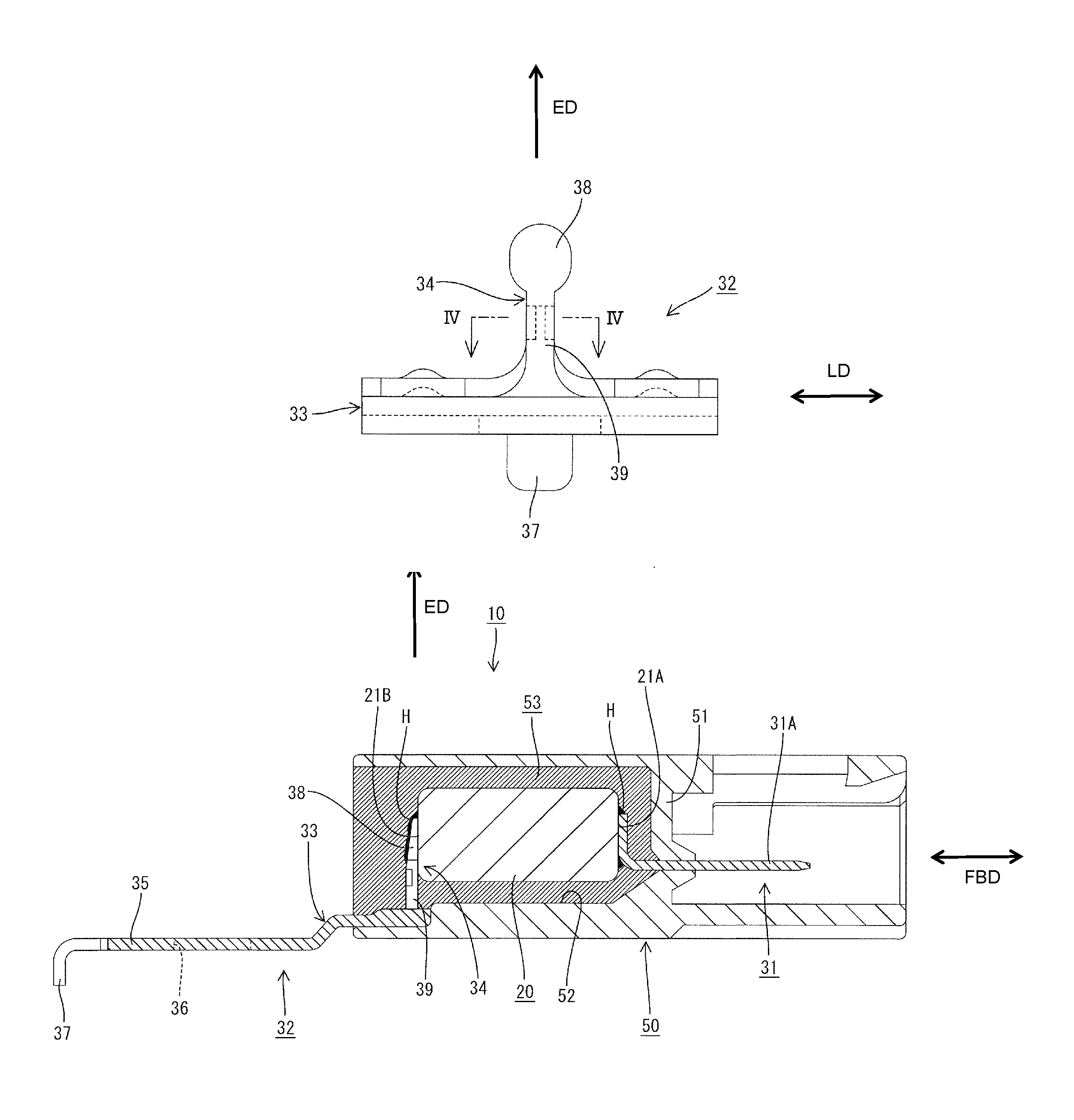
[0031]A connector in accordance with the illustrated embodiment of the invention is identified by the numeral 10 and has a built-in capacitor 20 as an electric or electronic device.

[0032]This connector 10 is provided for suppressing noise produced e.g. when a switch of an unillustrated defogger in a vehicle is turned on and off by grounding the defogger via the capacitor.

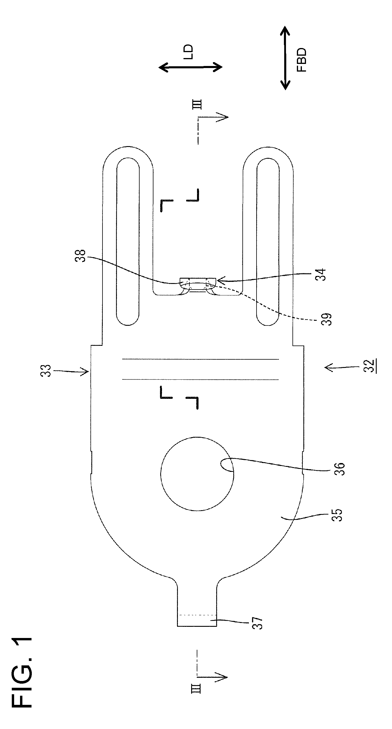
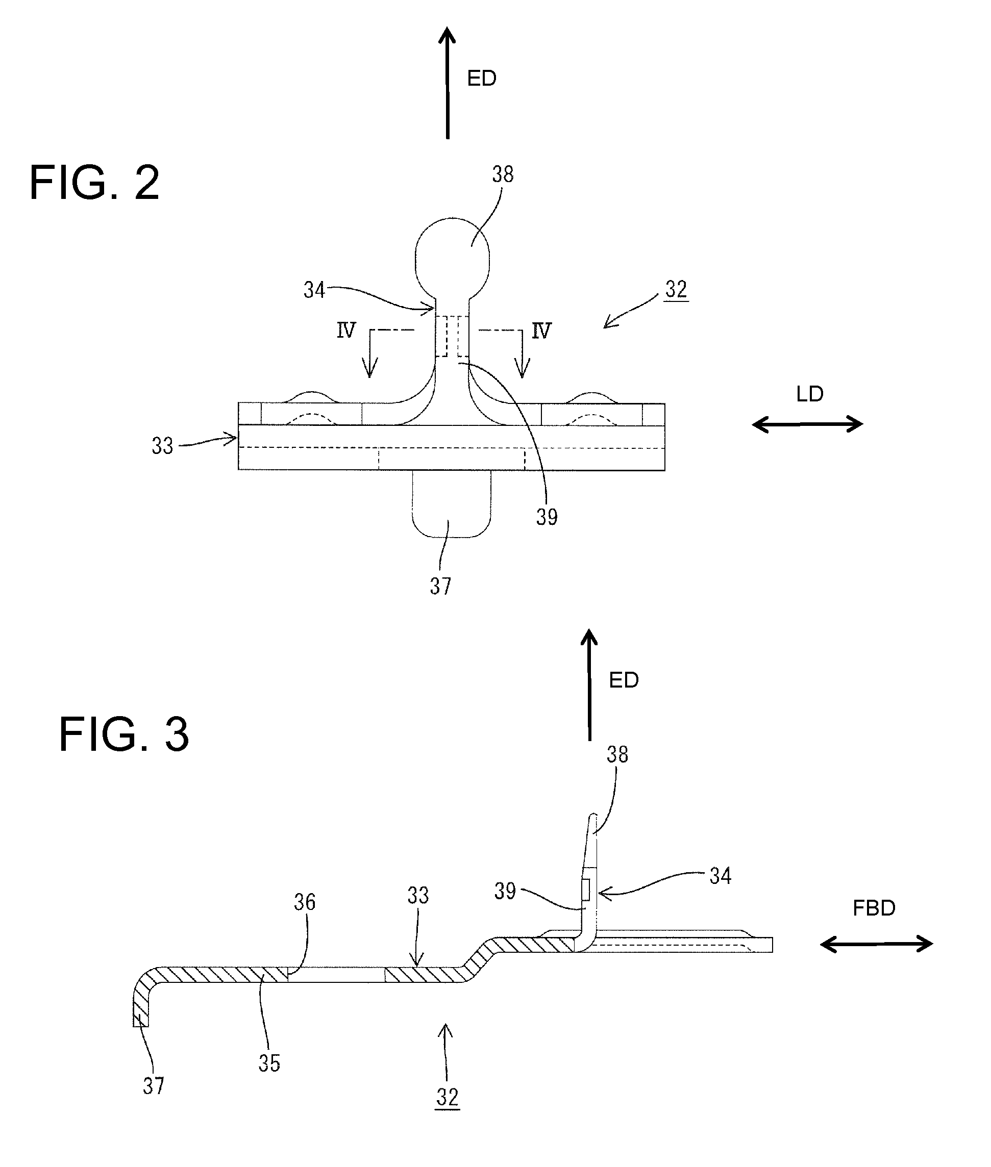
[0033]As shown in FIG. 7, the connector 10 includes the capacitor 20 extending in substantially forward and backward directions FBD, a wire-side terminal 31 to be connected to a wire-side electrode 21A on the front end of the capacitor 20, a ground-side terminal 32 to be connected to a ground-side electrode 21B on the rear end of the capacitor 20, a housing 50 made e.g. of synthetic resin and capable of accommodating the capacitor 20, and a molded portion 53 integrally covering the capacitor 20 connected to the wire-side terminal 31 and the ground-side terminal 32. Note that solder H is not shown in FIG. 5 to make c...


PUM


Abstract

A connector (10) has a capacitor (20) connected to a ground-side terminal (32) formed by press-working a metal base material in the form of a flat plate and is accommodated in a housing (50) made of synthetic resin. A connecting head (38) is provided on the ground-side terminal (32) and is thinner than the base material. The connecting head (38) is connected to a ground-side electrode (21B) provided on the capacitor (20) by soldering. A resiliently deformable neck (39) on the ground-side terminal (32) is narrower than the connecting head (38) and extends from the connecting head (38). A molded portion (53) is provided in the housing (50) to integrally cover the ground-side electrode (21B) of the capacitor (20) and the connecting head (38) of the ground-side terminal (32).

Description

BACKGROUND OF THE INVENTION[0001]1. Field of the Invention[0002]The present invention relates to a connector with a built-in electronic device.[0003]2. Description of the Related Art[0004]Japanese Unexamined Patent Publication No. 2006-173414 discloses a connector with a built-in capacitor as an electronic device. This connector is used to dispose a noise preventing capacitor at an intermediate position of a power supply line in the case of sharing a defogger equipped for a rear window of a vehicle with an antenna of a radio or the like. The connector includes two terminal fittings connected to two electrodes provided at both ends of the capacitor. A connector housing made of synthetic resin accommodates the capacitor and both terminal fittings. For example, this connector grounds the defogger to a body panel of the vehicle via the capacitor by connecting one terminal fitting to the defogger of the vehicle and bolting the other terminal fitting to the body panel. Thus, noise produce...

Claims


Application Information

Patent Timeline
Patent Type & Authority Patents(United States)
IPC IPC(8): H01R13/58
CPCH01R13/6625H01R43/20H01G4/228H01G2/04
Inventor FUJISAKI, RYUICHI
Owner SUMITOMO WIRING SYST LTD
Why Eureka
Try Eureka