Circuit board of LED lamp, LED lamp board and processing technology of circuit board

A production process and circuit board technology, which is applied in the direction of printed circuits, circuits, printed circuits, etc., where non-printed electrical components are connected, can solve the problems of poor welding performance, poor weldability, and long durability, and achieve good welding effect. High soldering temperature and high yield rate

Active Publication Date: 2014-12-03
深圳市鼎华芯泰科技有限公司
View PDF6 Cites 1 Cited by
  • Summary
  • Abstract
  • Description
  • Claims
  • Application Information

AI Technical Summary

Problems solved by technology

However, the welding performance of aluminum materials is poor, the pulling force is weak when the aluminum leads and the aluminum wafer sub-seat are ultrasonically welded, the feasibility of connecting the aluminum leads is poor, the excellent rate of the LED light board is low, and it is easy to use. malfunction
In addition, the solderability between the aluminum power line pads of the circuit board and the copper power line is poor. Although solder paste can be used to achieve welding between copper wires and aluminum pads, the reliability of the joints is poor, and the risk of durability is greater.

Method used


Image

  • Circuit board of LED lamp, LED lamp board and processing technology of circuit board
  • Circuit board of LED lamp, LED lamp board and processing technology of circuit board
  • Circuit board of LED lamp, LED lamp board and processing technology of circuit board

Examples


Embodiment 1

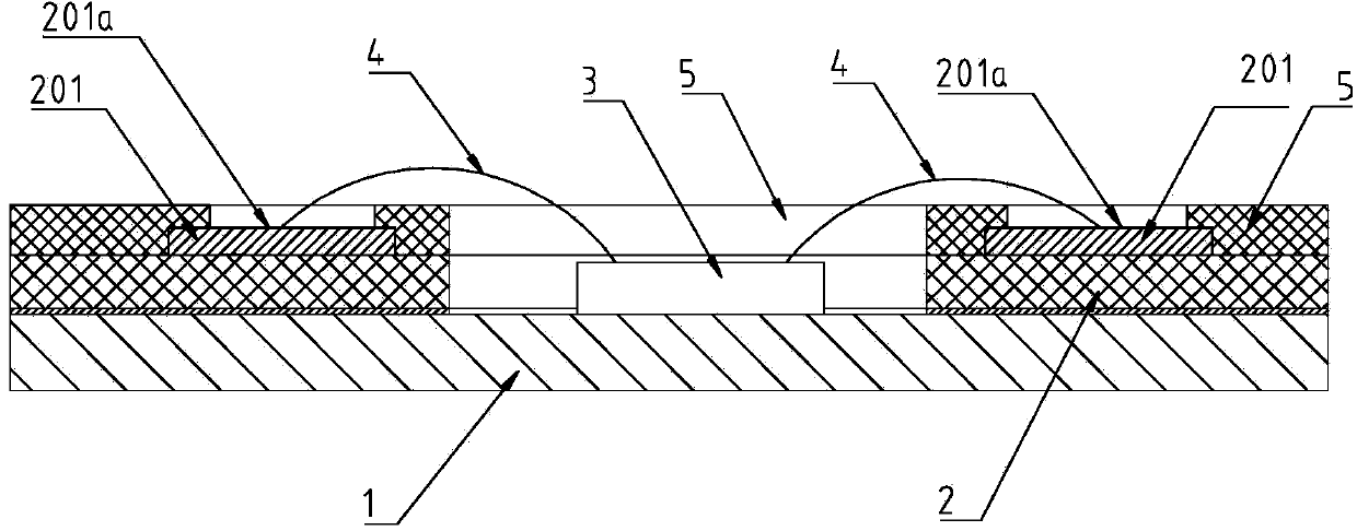
[0074] Conductive lines are formed on the surface of the board. After sandblasting, a solder mask is applied, and holes for welding wafers are drilled. The steps are as follows:

[0075] 1) Select an aluminum-silicon alloy foil plate with a thickness of 0.1mm (aluminum 40μm / insulation layer 50μm / glue 10μm) and cut it to the required size;

[0076] 2) After the board surface is cleaned, directly print the conductive circuit pattern of acid-resistant ink, and bake in an oven at 70°C for 30 minutes;

[0077] 3) After etching and removing the film, the conductive lines required for the circuit design are formed;

[0078] 4) Make an on-off test, there is no open and short circuit phenomenon, which meets the circuit design requirements;

[0079] 5) On the surface of the aluminum-silicon alloy foil plate forming the conductive circuit, do a sandblasting treatment; the sandblasting parameters are:

[0080] Sand blasting machine: JYN1121 (Shenzhen Juyongneng Technology Co., Ltd.)

...

Embodiment 2

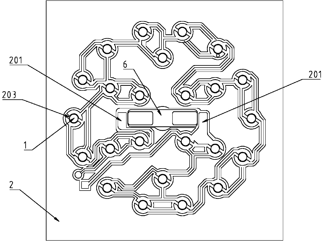
[0099] The production process of aluminum-silicon alloy foil board adopts the method of first transferring the conductive circuit pattern on the board surface image, then drilling the hole for welding the wafer, then etching, removing the film, and finally attaching the gold-plated pad, and the reflective white film, pressing and then drilling Screw holes and wire holes, the steps are as follows:

[0100] 1) Select an aluminum-silicon alloy foil plate with a thickness of 0.1mm (aluminum 40μm / insulation layer 50μm / glue 10μm) and a reflective white film with a thickness of 0.1mm, and cut it into the required size;

[0101] 2) After the board surface is cleaned, directly print the conductive circuit pattern of acid-resistant ink, and bake in an oven at 70°C for 30 minutes;

[0102] 3) According to the circuit design, drill holes at the position where the wafer needs to be welded; at the same time, drill the cut reflective white film according to the position of the soldered wafer...

Embodiment 3

[0122] The production process of aluminum-silicon alloy foil board adopts the method of first transferring the conductive circuit pattern on the board surface, then drilling the holes for soldering wafers, then etching, removing the film, and finally pasting the copper pad, and the reflective white film, and then laminating it. Drill screw holes and cable holes, the steps are as follows:

[0123] 1) Select an aluminum-silicon alloy foil plate with a thickness of 0.1mm (aluminum 40μm / insulating layer 50μm / glue 10μm) and a reflective white film of 0.1mm, and cut it into the required size;

[0124] 2) After the board surface is cleaned, directly print the conductive circuit pattern of acid-resistant ink, and bake in an oven at 70°C for 30 minutes;

[0125] 3) According to the circuit design, drill holes at the position where the wafer needs to be welded; at the same time, drill the cut reflective white film according to the position of the soldered wafer and the positive and nega...


PUM


Abstract

The invention discloses a circuit board of an LED lamp, an LED lamp board and a processing technology of the circuit board. The LED lamp board includes LED wafers, wafer lead wires and the circuit board. The circuit board includes mirror boards, a substrate and a solder mask layer. The substrate includes wafer installation holes. The mirror boards are bonded on the back of the substrate. The solder mask layer covers the front face of the substrate. The front face of the substrate includes aluminum conductive lines. The outer surfaces of the conductive lines include abrasive blasting rough layers. The wafer lead wires are ultrasonically welded with bonding pads on the aluminum conductive lines of the circuit board. The LED wafers are pasted on the mirror boards in the wafer installation holes of the substrate. The outer surfaces of the conductive lines are provided with the rough layers formed through abrasive blasting, and during ultrasonic welding with metal lead wires, especially aluminum lead wires, the fusion degree of the lead wires and the bonding pads is high. Compared with aluminum alloy bonding pads which do not undergo the abrasive blasting processing, the lead wires are capable of bearing a higher tension. The manufactured LED lamp board is high in good rate and low in fault rate in a use process.

Description

[technical field] [0001] The invention relates to LED lighting, in particular to a circuit board of an LED lamp, an LED lamp board and a production process for the circuit board. [Background technique] [0002] Due to the characteristics of energy saving, low consumption, and long life, LEDs are widely used as lighting sources, and are still developing rapidly. Common LED lighting is usually a white light, and some are directly sealed with chips. At present, there is a situation of decreasing brightness of white light, especially when the power is higher, this problem will be more prominent; and when the current is increased, the thermal resistance of the packaging material will drop below 10K / W, and the packaging material is generally epoxy resin. After the thermal resistance is reduced, the heat dissipation effect from the package to the PCB board will be reduced, resulting in an increase in the temperature of the LED chip and a decrease in luminous efficiency. Although ...

Claims


Application Information

Patent Timeline
Patent Type & Authority Applications(China)
IPC IPC(8): H05K1/18H05K3/02H05K3/46H01L33/48H01L33/62
CPCH01L2224/48091
Inventor 何忠亮殷和斌丁华沈正叶文黄俊河沈洁
Owner 深圳市鼎华芯泰科技有限公司
Why Eureka
Try Eureka