Display panel and manufacturing method thereof

a technology of display panel and manufacturing method, which is applied in the field of display panel, can solve the problems of limited space utilization, considerable energy consumption, and inability to be perfect choices for users, and achieve the effects of preventing the polluting of the display medium layer in the display region, widening the sealant, and reducing the size of the display panel

Active Publication Date: 2014-01-07
AU OPTRONICS CORP
View PDF13 Cites 2 Cited by
  • Summary
  • Abstract
  • Description
  • Claims
  • Application Information

AI Technical Summary

Benefits of technology

[0005]The present invention provides a display panel which includes a sealant having sufficient tensile strength and accurate width control.
[0006]The present invention also provides a manufacturing method of display panel, the manufacturing method gives consideration to tensile strength of a sealant and accuracy of width control, thereby improving process yield.
[0022]In the present invention, the width of the sealant is increased from the side of the sealant away from the display region, so that the maximum width of the corner portion of the sealant is larger than the widths of the strip-shaped portions. Therefore, tensile strength of the sealant is promoted. The sealant can be avoided from spanning or being too close to the display region, and thereby the display medium layer in the display region can be prevented from being polluted.

Problems solved by technology

However, it may not be a perfect choice for a user who simultaneously operates several computer terminals / displays, or from the view of environmental protection.
In view of the energy saving trend, the CRT has many problems, such as limited space utilization and considerable energy consumption.
In particular, the CRT is not capable of providing a solution to meet the light, slim, short and small tendency today and the demand on low power consumption.

Method used


Image

  • Display panel and manufacturing method thereof
  • Display panel and manufacturing method thereof
  • Display panel and manufacturing method thereof

Examples


Embodiment Construction

[0040]The present invention will now be described more specifically with reference to the following embodiments. It is to be noted that the following descriptions of preferred embodiments of this invention are presented herein for purpose of illustration and description only. It is not intended to be exhaustive or to be limited to the precise form disclosed.

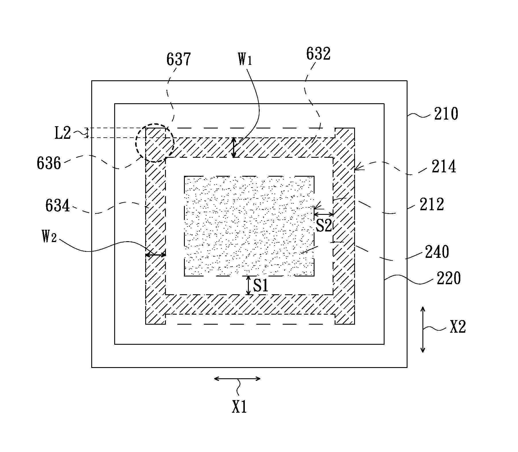
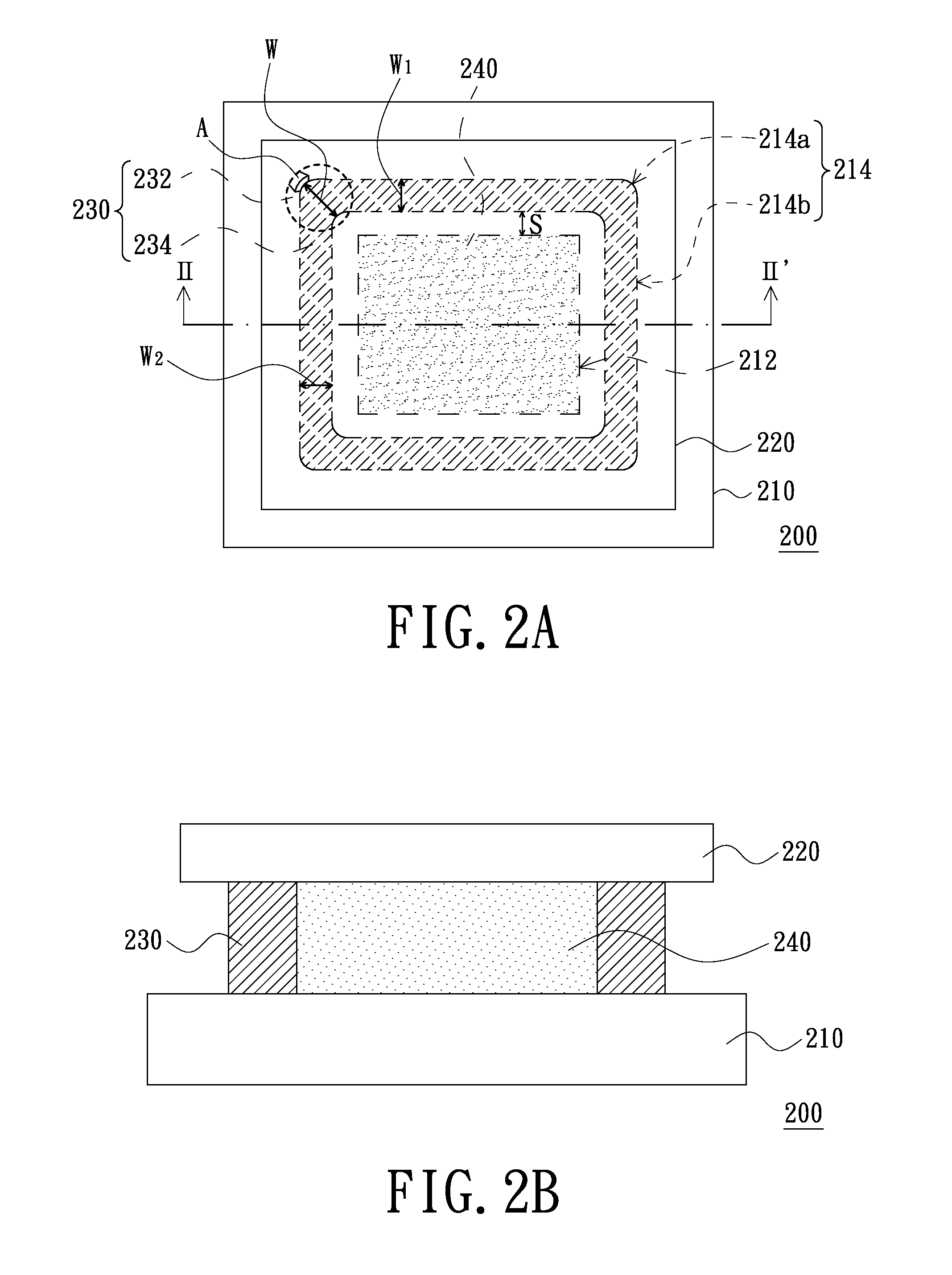
[0041]FIG. 2A is a schematic, top view of a display panel according to an embodiment of the present invention, and FIG. 2B is a schematic, cross-sectional view of the liquid crystal display panel of FIG. 2A, taken along a line II-II′. Referring to FIG. 2A and FIG. 2B, a liquid crystal display panel 200 includes a first substrate 210, a second substrate 220 and a sealant 230, wherein the first substrate 210 has a display region 212 and a sealant coating region 214, and the sealant coating region 214 surrounds the display region 212. A pixel array (not shown) of the liquid crystal display panel 200 is disposed in the display region...


PUM

PropertyMeasurementUnit
widthsaaaaaaaaaa
widths W1aaaaaaaaaa
speedaaaaaaaaaa

Abstract

A display panel includes a first substrate, a second substrate and a sealant. The first substrate has a display region and a sealant coating region, the sealant coating region surrounds the display region. The second substrate is disposed above the first substrate. The sealant is disposed between the first substrate and the second substrate and is located in the sealant coating region. The sealant includes at least one corner portion and a plurality of strip-shaped portions. The adjacent strip-shaped portions intersect at the corner portion, and a maximum width of the corner portion is larger than widths of the strip-shaped portions. A manufacturing method of the display panel is also provided.

Description

FIELD OF THE INVENTION[0001]The present invention relates to a display panel and a manufacturing method thereof, and more particularly to a display panel having a narrow bezel and a manufacturing method thereof.BACKGROUND OF THE INVENTION[0002]The rapid progress of science and technology in modern society largely benefits from the rapid progress of semiconductor components or human-machine display devices. Because of its excellent display quality and economic advantage, cathode ray tubes (CRTs) have dominated the market in recent years. However, it may not be a perfect choice for a user who simultaneously operates several computer terminals / displays, or from the view of environmental protection. In view of the energy saving trend, the CRT has many problems, such as limited space utilization and considerable energy consumption. In particular, the CRT is not capable of providing a solution to meet the light, slim, short and small tendency today and the demand on low power consumption....

Claims


Application Information

Patent Timeline
Patent Type & Authority Patents(United States)
IPC IPC(8): G02F1/1339
CPCG02F1/1339
Inventor YANG, WEI-CHIEHCHIEN, WEI-YIHUANG, YU-RUNG
Owner AU OPTRONICS CORP
Why Eureka
Try Eureka