Hybrid silicon wafer
a hybrid silicon and silicon wafer technology, applied in the field of hybrid silicon wafers, can solve the problems of increasing the cost of the lsi process, the size of the monocrystalline wafer, and the cost of the dummy wafer, so as to improve the production yield, improve the strength, and facilitate the processing of complex shapes
- Summary
- Abstract
- Description
- Claims
- Application Information
AI Technical Summary
Benefits of technology
Problems solved by technology
Method used
Image

Examples
example 1
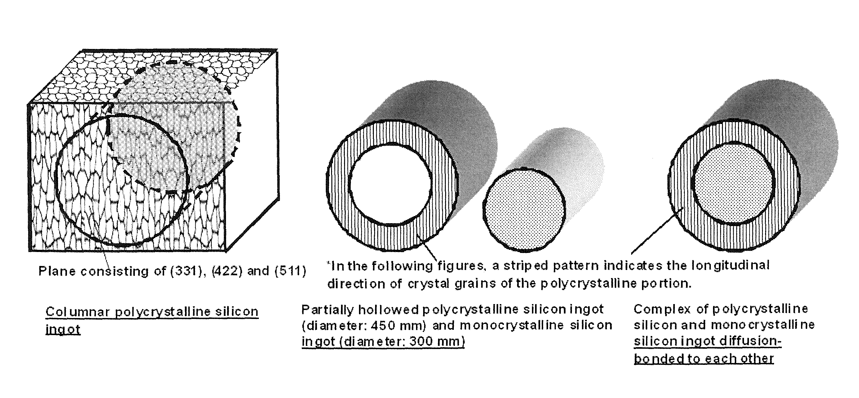
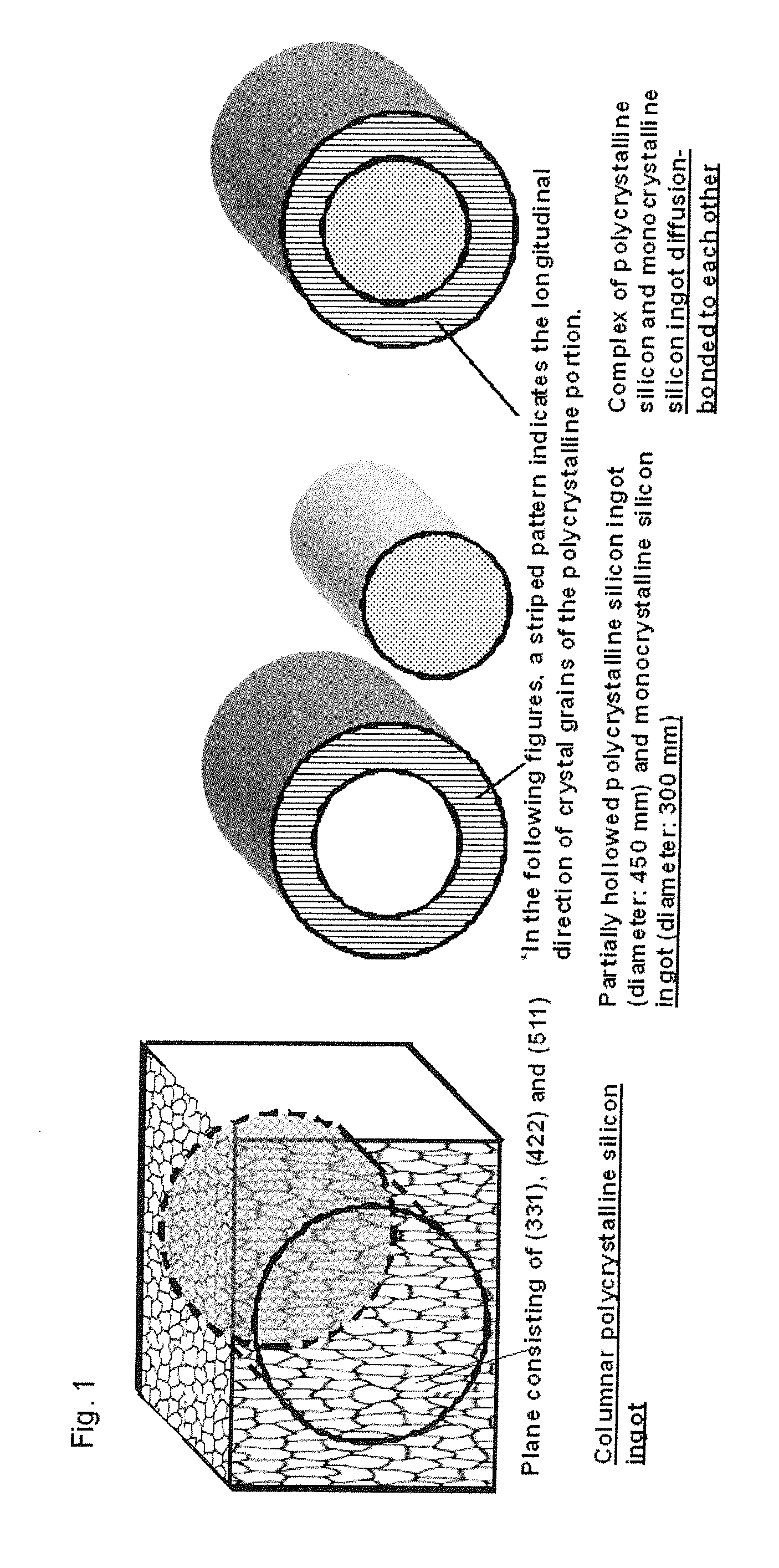
[0060]Based on the unidirectional solidification / melting method, prepared was a columnar structure polycrystalline silicon ingot wherein the purity is 6N, the impurity concentration of Cu, Fe, Ni, and Al is 0.1 ppm or less, respectively, and the oxygen and carbon content is 100 ppm or less. In the foregoing case, the plane direction of the columnar structure polycrystalline silicon that was prepared by the unidirectional solidification / melting method consisted of (331), (422), and (511). Moreover, in this Example, in order to increase the purity of the polycrystalline silicon portion as much as possible, used was a raw material in which the purity excluding gas components is 6N or higher, the total amount of metal impurities is 1 wtppm or less, and, among the metal impurities, Cu, Fe, Ni, and Al are respectively 0.1 wtppm or less, and C and O as gas components are respectively 100 wtppm or less.
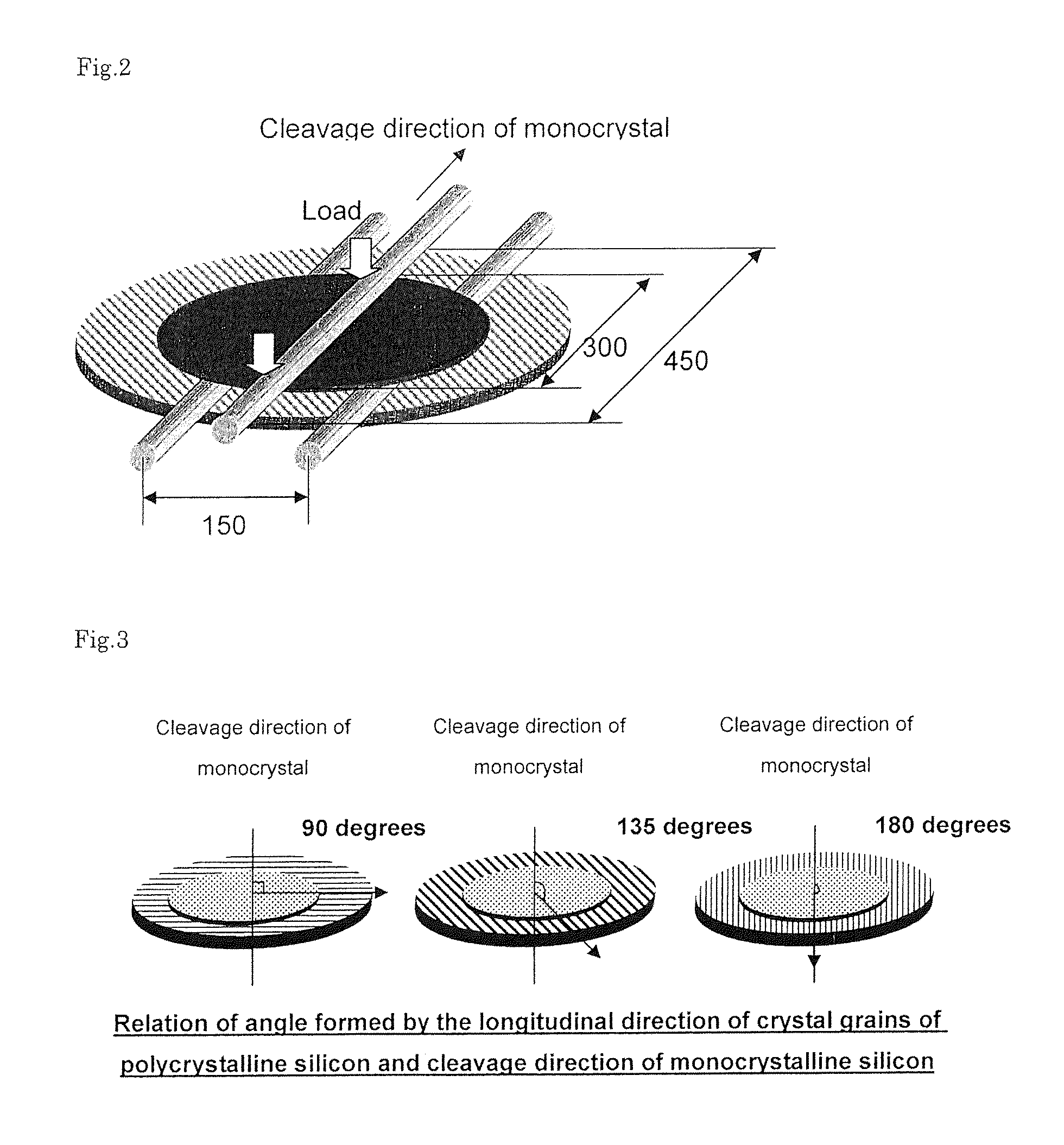
[0061]Subsequently, as shown in FIG. 1, this polycrystalline silicon (diameter of 450 mm)...
example 2
[0073]Prepared was a hybrid silicon wafer in which Cu and Fe as impurities in the polycrystalline silicon portion were respectively 0.5 wtppm and 0.3 wtppm, Ni and Al were respectively 0.1 wtppm or less, and the purity excluding gas components was 6N or higher.
[0074]In the foregoing case, upon conducting a thermal transfer test in order to examine the influence of Cu and Fe as impurities, transfer of Cu and Fe to the contacted monocrystalline wafer was observed. Accordingly, this cannot be used as a dummy wafer for use in a process including heat treatment at a high temperature.
[0075]However, the influence of Cu and Fe as impurities was not that significant, and this could be sufficiently used as a dummy wafer in a process that does not include heat treatment at a high temperature.
example 3
[0076]Prepared was a hybrid silicon wafer in which Cu, Fe, Ni, and Al as impurities in the polycrystalline silicon portion were respectively 0.8 wtppm, 1.2 wtppm, 0.3 wtppm, and 0.6 wtppm, and the purity excluding gas components was 5N or higher.
[0077]In the foregoing case, upon conducting a thermal transfer test in order to examine the influence of Cu, Fe, Ni, and Al as impurities, transfer of Cu, Fe, Ni, and Al to the contacted monocrystalline wafer was observed. However, the transfer of other impurities could not be observed.
[0078]Accordingly, this cannot be used as a dummy wafer for use in a process including heat treatment at a high temperature. However, the influence of Cu, Fe, Ni, and Al as impurities was not that significant, and this could be sufficiently used as a dummy wafer in a process that does not include heat treatment at a high temperature.
[0079]Based on foregoing Example 2 and Example 3, for use as a dummy wafer in a process including heat treatment at a high tempe...
PUM
| Property | Measurement | Unit |
|---|---|---|
| angle | aaaaa | aaaaa |
| diameter | aaaaa | aaaaa |
| inner diameter | aaaaa | aaaaa |
Abstract
Description
Claims
Application Information
 - R&D Engineer
- R&D Manager
- IP Professional
- Industry Leading Data Capabilities
- Powerful AI technology
- Patent DNA Extraction
Browse by: Latest US Patents, China's latest patents, Technical Efficacy Thesaurus, Application Domain, Technology Topic.
© 2024 PatSnap. All rights reserved.Legal|Privacy policy|Modern Slavery Act Transparency Statement|Sitemap