
Validation of integrated circuit designs built with encrypted silicon IP blocks

Active Publication Date: 2014-03-04
ENCRIP
View PDF5 Cites 7 Cited by
  • Summary
  • Abstract
  • Description
  • Claims
  • Application Information

AI Technical Summary

Benefits of technology

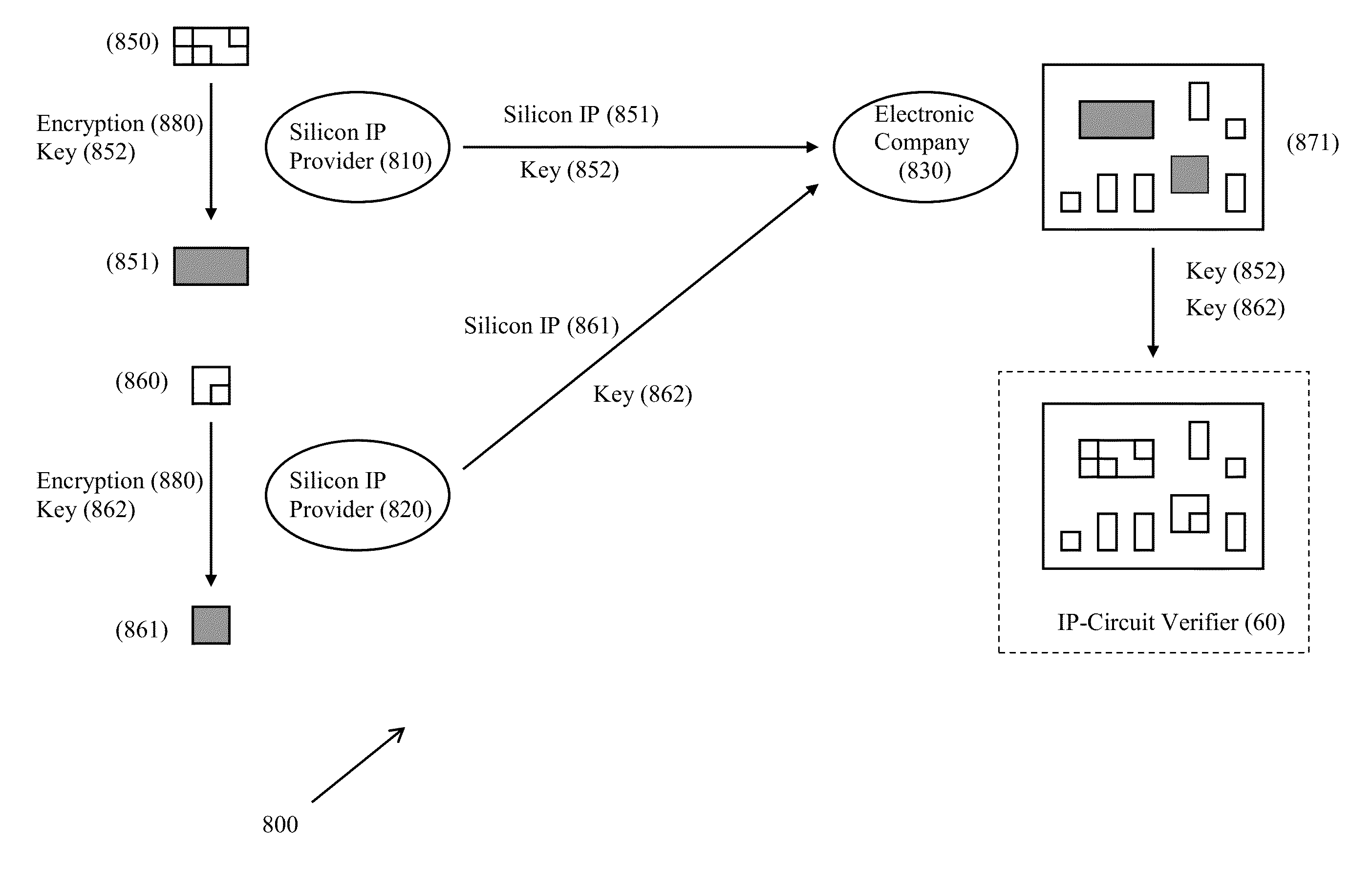
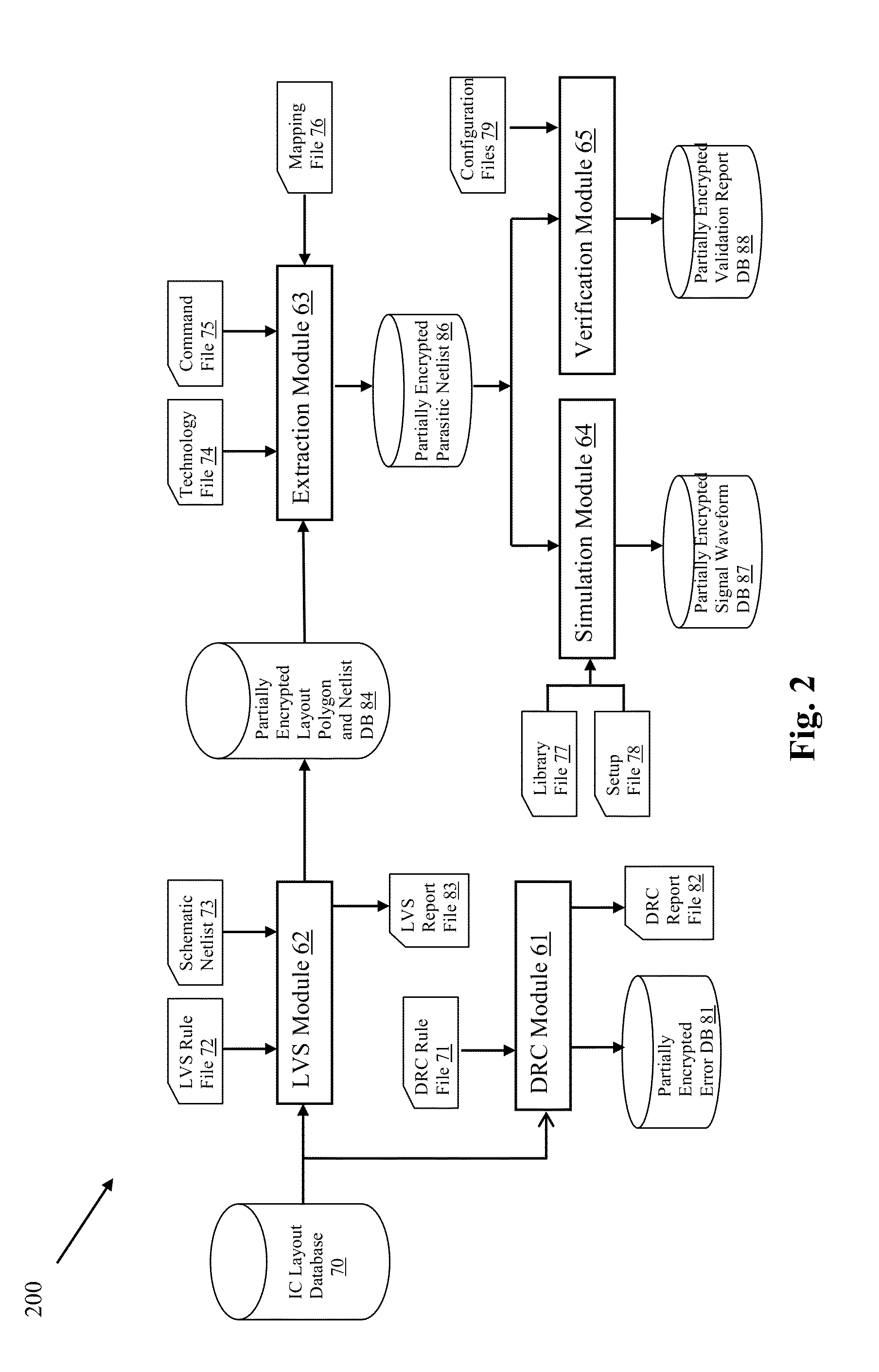
The present invention provides a method and system for validating integrated circuit designs that use encrypted silicon IP blocks. The method involves reading and decrypting the layout database file and the technology file to get a circuit network consisting of nets, devices, and RCs. The method also includes performing design rule checks, LVS checks, and signal waveform simulation checks. The system includes a DRC module, an LVS module, an extraction module, a simulation module, and other validation modules. The technical effect of the invention is to provide a more efficient and effective way of validating integrated circuit designs that use encrypted silicon IP blocks.

Problems solved by technology

Then, it does design rule checks on the polygons and texts and finds rule violations.

Method used


Image

  • Validation of integrated circuit designs built with encrypted silicon IP blocks
  • Validation of integrated circuit designs built with encrypted silicon IP blocks
  • Validation of integrated circuit designs built with encrypted silicon IP blocks

Examples


Embodiment Construction

[0033]U.S. Pat. No. 8,117,661, “Encryption based silicon IP protection”, issued Feb. 14, 2012, to the present inventor, Weidong Zhang, describes many of the underlying concepts, methods, and systems that can be usefully employed here. Such Patent is incorporated herein, in full.

[0034]In one or more embodiments as described herein, a method and system for validating an integrated circuit design, built with encrypted silicon IP blocks, is provided, wherein DRC and LVS check, parasitic RC extraction, circuit simulation and other circuit validation checks, such as signal EM (Electro migration) and voltage drop check, SI (Signal Integrity) check and static timing check, etc. are performed.

[0035]In the following detailed description, references are made to the accompanying drawings that form a part hereof, and in which are shown by way of illustration specific embodiments or examples.

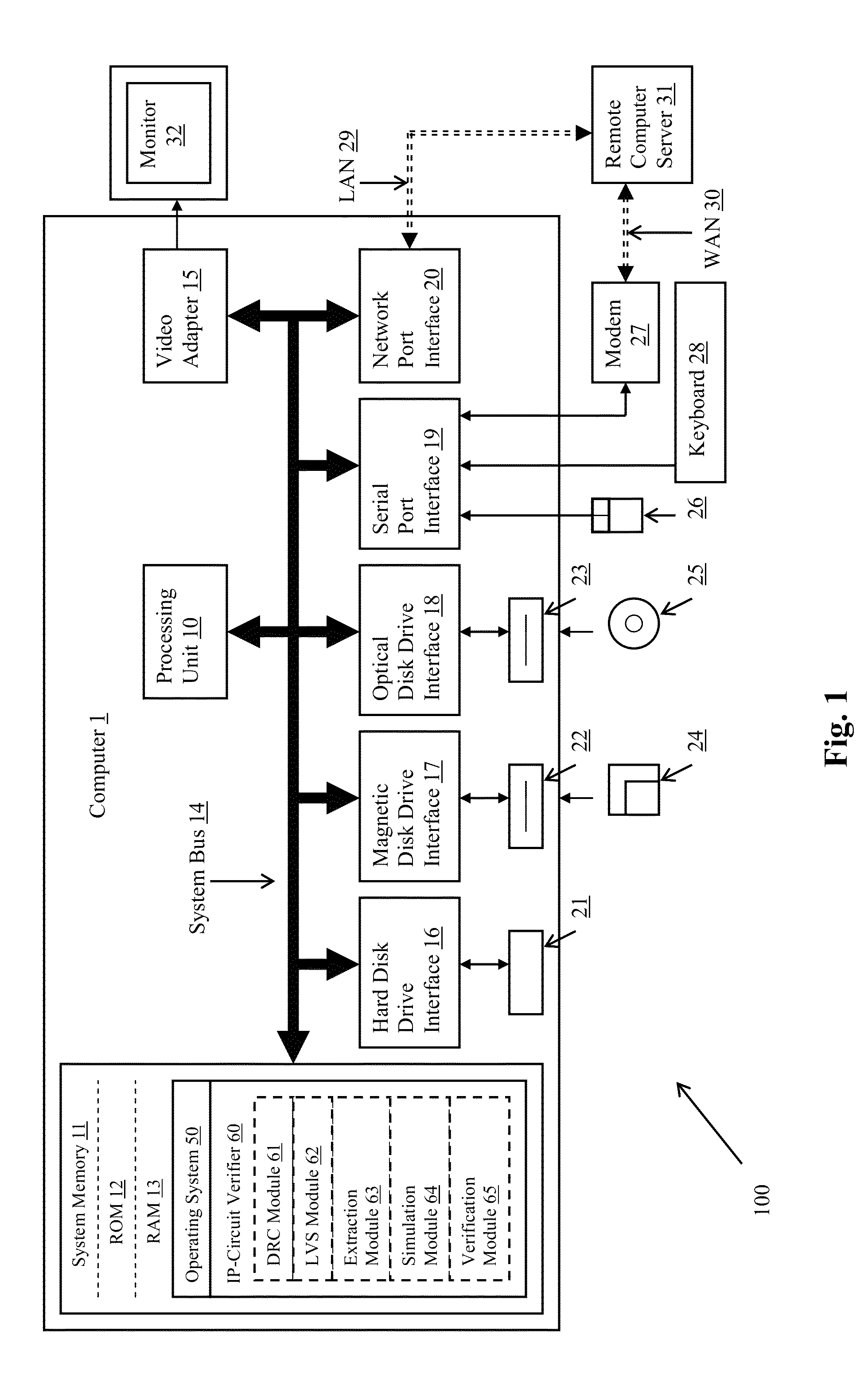
[0036]FIG. 1 represents a general purpose computer system or network 100 capable of hosting an IP circuit ...


PUM


Abstract

A method and system for validating integrated circuit designs that are built with encrypted silicon IP blocks decrypts the encrypted silicon IP blocks in the integrated circuit designs with the keys from IP providers. After decryption, various validation checks on the integrated circuit designs are done, such as design rule check (DRC), layout versus schematic (LVS) check, parasitic resistor capacitor (RC) extraction, circuit simulation, signal electro migration (EM) and voltage drop check, signal integrity (SI) check and static timing check, etc. After validation, any confidential data from the checking results related to the encrypted silicon IP blocks are themselves encrypted to protect the proprietary silicon IP blocks. The method and system work with silicon IP encryption technology to establish a low cost silicon IP usage and verification platform, and to enable a more cost efficient silicon IP business model.

Description

BACKGROUND OF THE PRESENT INVENTION[0001]I. Technical Field[0002]The present invention relates to validating integrated circuit designs built with encrypted silicon IP blocks. Furthermore, the present invention relates to establishing a low cost silicon IP usage and verification platform.[0003]II. Background[0004]Modern electronics circuit designs are now so complex that circuit designers had to resort to computer system-aided design tools to complete the circuit designs in reasonable time frames. Once a design is committed to silicon production, it's too late and too expensive to even consider not getting it right the first time. In the past, the first production prototypes were debugged in target hardware. Now with computer system aided design tools, the circuits can be simulated and checked while still only manifested as software in design files.[0005]As recently as 20-30 years ago, whole functional parts like printer controllers, direct memory access controllers, serial data inp...

Claims


Application Information

Patent Timeline
Patent Type & Authority Patents(United States)
IPC IPC(8): G06F17/50
CPCG06F17/50G06F17/5081G06F30/398
Inventor WANG, TONGSHENGZHANG, WEIDONG
Owner ENCRIP
Learn More