3D inter-stratum connectivity robustness

a connectivity robustness and interstratum technology, applied in the field of integrated circuits, can solve the problems of unintentional shorting of interface signals, clocks or powers to each other, or left unconnected, and achieve the effect of not being electrically connected, open, and the same net from two face-to-face or face-to-back strata

Active Publication Date: 2013-02-19
GLOBALFOUNDRIES US INC
View PDF63 Cites 9 Cited by
  • Summary
  • Abstract
  • Description
  • Claims
  • Application Information

AI Technical Summary

Benefits of technology

[0007]According to an aspect of the present principles, there is provided a method for verifying inter-stratum connectivity for two or more strata to be combined into a 3D chip stack. Each of the two or more strata has 3D elements including active 3D elements, mechanical 3D elements, and dummy 3D elements. The method includes performing a respective 2D layout ver

Problems solved by technology

In 3D stacked integrated circuit assemblies, however, there are scenarios where, even with each chip passing its own LVS and methodology checks, the interface signals, clocks or powers can be unintentionally shorted to each other or left unconnected (open) when all chips are

Method used


Image

  • 3D inter-stratum connectivity robustness
  • 3D inter-stratum connectivity robustness
  • 3D inter-stratum connectivity robustness

Examples


Embodiment Construction

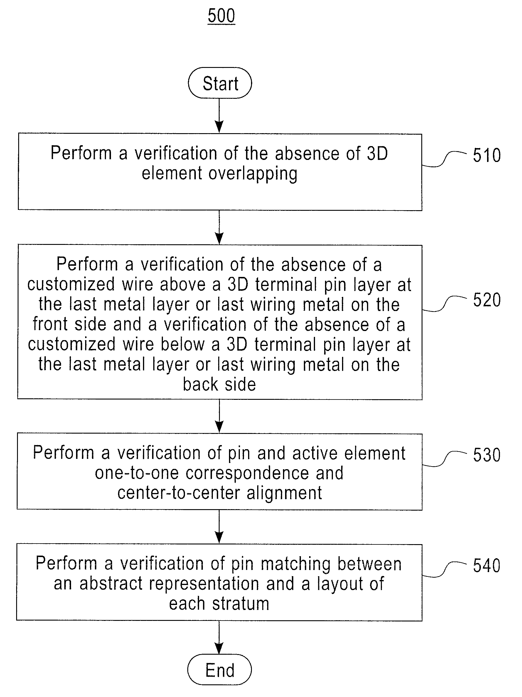
[0024]The present principles are directed to 3D inter-stratum connectivity robustness.

[0025]Advantageously, the present principles provide a novel design methodology to ensure that in 3D stacked integrated circuit (IC) technology, the circuits, macros, units, and chips are functionally connected between adjacent silicon layers (strata) using various 3D elements such as TSVs (through-silicon vias) and micro / mini C4 (a smaller version of the inter-chip C4s) connections (collectively referred to hereinafter as simply “C4 connections”). A set of design methodology rules is provided to achieve robust physical verification of 3D stacked IC interconnections insuring no signal or power terminals are shorting or unconnected within these 3D assemblies, i.e., the 3D layout versus the schematic is (LVS) clean. “LVS” clean refers to the situation where a particular integrated circuit layout corresponds to (i.e., matches) the original schematic or circuit diagram of the design. Usually, the match...


PUM


Abstract

There is provided a method for verifying inter-stratum connectivity for two or more strata to be combined into a 3D chip stack. Each of the two or more strata has 3D elements including active 3D elements, mechanical 3D elements, and dummy 3D elements. The method includes performing a respective 2D layout versus schematic verification on each of the two or more strata with respect to at least the 3D elements to pre-ensure an absence of shorts between the 3D elements when the two or more strata are subsequently stacked into the 3D chip stack. The method further includes checking inter-stratum interconnectivity between each adjacent pair of strata in the 3D chip stack.

Description

CROSS-REFERENCE TO RELATED APPLICATIONS[0001]This application is related to the following commonly assigned applications, all concurrently filed herewith and incorporated herein by reference: Ser. No. 13 / 217,734, entitled “PROGRAMMING THE BEHAVIOR OF INDIVIDUAL CHIPS OR STRATA IN A 3D STACK OF INTEGRATED CIRCUITS”; Ser. No. 13 / 217,335, entitled “SYNCHRONIZING GLOBAL CLOCKS IN 3D STACKS OF INTEGRATED CIRCUITS BY SHORTING THE CLOCK NETWORK”; Ser. No. 13 / 217,349, entitled “3D CHIP STACK SKEW REDUCTION WITH RESONANT CLOCK AND INDUCTIVE COUPLING”; Ser. No. 13 / 217,767, entitled “3D INTEGRATED CIRCUIT STACK-WIDE SYNCHRONIZATION CIRCUIT”; Ser. No. 13 / 217,789 entitled “CONFIGURATION OF CONNECTIONS IN A 3D STACK OF INTEGRATED CIRCUITS”; Ser. No. 13 / 217,406, entitled “AC SUPPLY NOISE REDUCTION IN A 3D STACK WITH VOLTAGE SENSING AND CLOCK SHIFTING”; and Ser. No. 13 / 217,429, entitled “VERTICAL POWER BUDGETING AND SHIFTING FOR 3D INTEGRATION”.BACKGROUND[0002]1. Technical Field[0003]The present in...

Claims


Application Information

Patent Timeline
IPC IPC(8): G06F17/50
CPCG06F17/5081H01L25/0657G06F2217/40H01L2924/0002H01L2924/00G06F30/398G06F2113/18
Inventor BEAKES, MICHAEL P.LO, SHIH-HSIENSCHEUERMANN, MICHAEL R.WORDEMAN, MATTHEW R.
Owner GLOBALFOUNDRIES US INC
Why Eureka
Try Eureka