Method for manufacturing semiconductor device and semiconductor wafer
a manufacturing method and technology for semiconductor devices, applied in semiconductor devices, semiconductor/solid-state device details, electrical devices, etc., can solve problems such as metal contamination and metal contamination
- Summary
- Abstract
- Description
- Claims
- Application Information
AI Technical Summary
Benefits of technology
Problems solved by technology
Method used
Image

Examples
example 1
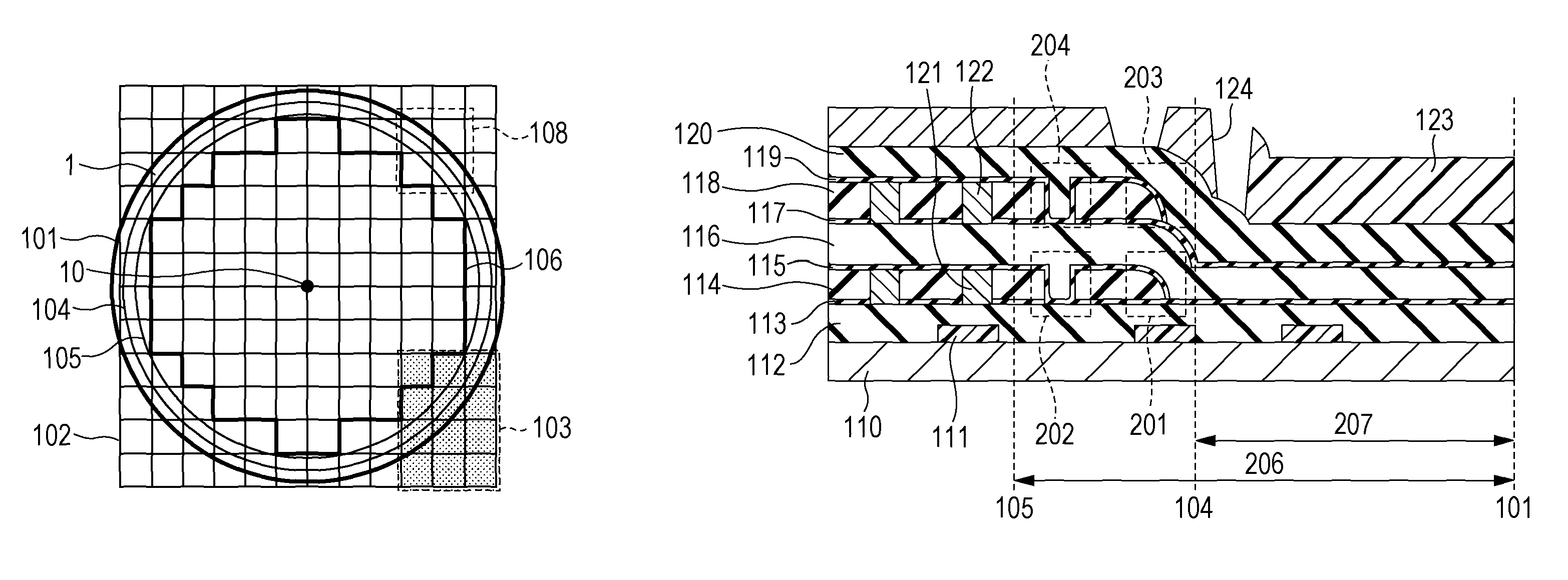
[0038]Example 1 is described with reference to FIG. 1A to FIG. 6C. First, the subject of the invention is described in more detail with reference to FIGS. 1A to 1C.
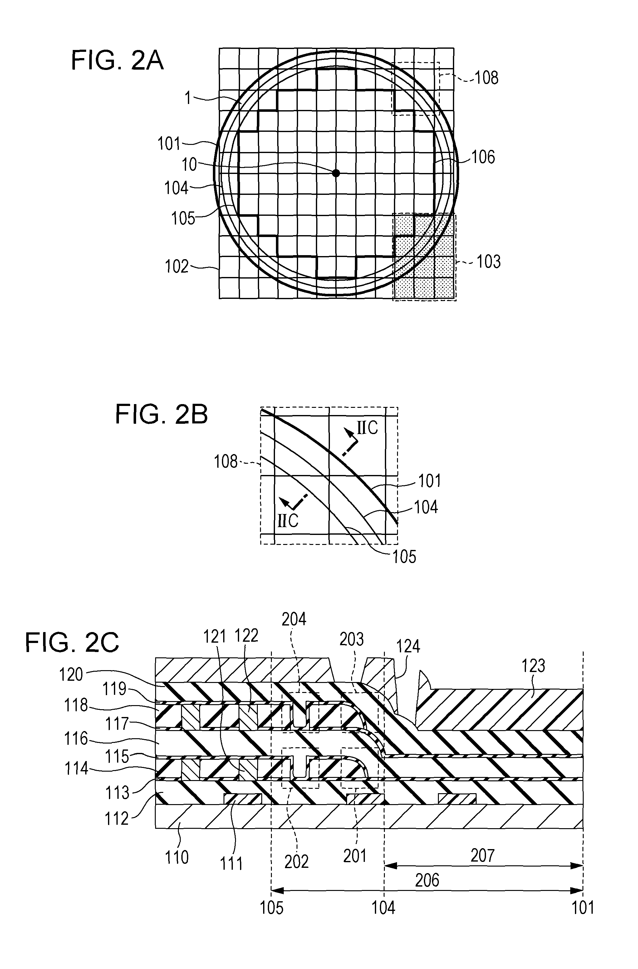
[0039]FIG. 1A is a plan schematic view of a semiconductor wafer 1 (hereinafter also referred to as a wafer) and an exposure region. FIG. 1A is a plan view as viewed from directly above a center 10 of the wafer 1 to the principal surface which is an element formation surface of the wafer. A circumference 101 of the wafer is the circumference of the wafer 1 and the outer edge of the principal surface of the wafer 1. FIG. 1A illustrates lattices for describing the exposure region. An exposure region 103 illustrates a range which is irradiated with exposure light in one exposure process. More specifically, a region corresponding to the 3×4 lattices is exposed in one exposure process. Although described in detail later, in this example, the exposure refers to exposure in a process of forming a mask pattern for etching (a certa...
example 2
[0068]This Example is described with reference to FIGS. 7A and 7B. Example 2 is different from Example 1 in that this example has a configuration in which an optical waveguide is not provided and a through hole via is provided and other configurations are the same as those of Example 1. FIG. 7A and FIG. 7B of this example illustrate a configuration corresponding to FIG. 5A and FIG. 5B of Example 1. The same configurations are designated by the same reference numerals and the description thereof is omitted.
[0069]In FIG. 7A, a mask 701 containing photoresist is provided. The mask 701 can be formed by exposure in the exposure region 103 illustrated in FIG. 2A of Example 1. The mask 701 has openings 702 for a through hole via or a through hole electrode. The through hole via or the through hole electrode contains a conductor formed by penetrating a plurality of insulation films and is used for connecting an external pad portion to which an external terminal is connected and a semiconduc...
example 3
[0071]This example is described with reference to FIGS. 8A to 8D. This example describes a configuration when wiring is further added to the configuration of Example 1 and other configurations are the same as those of Example 1. FIG. 8A to FIG. 8D of this example are cross sectional views for describing a manufacturing method continuous to FIG. 6A of Example 1. The same configurations as those of FIG. 6A are designated by the same reference numerals and the description thereof is omitted.
[0072]The insulation film 601 and the high refractive-index film 603 of FIG. 6A are partially removed to form a high refractive-index film 801 and an insulation film 802 (FIG. 8A). Then, an insulation film 803 containing silicon oxide, for example, is formed. The insulation film 803 buries the high refractive-index film 801 and the insulation film 802 and has a flat upper surface which has been subjected to planarization treatment (FIG. 8B). Then, openings are formed in the insulation film 803 and p...
PUM
 Abstract
Description
Claims
Application Information