Method for formation of an electrically conducting through via

a technology of electrical conductance and via, which is applied in the direction of electrical apparatus, semiconductor devices, and testing/measurement of semiconductor/solid-state devices, etc., can solve the problems of difficult to implement fabrication steps at high temperatures, damage to integrated circuits, and approach may have temperature limitations, so as to achieve easy fracture

Active Publication Date: 2014-03-18
STMICROELECTRONICS (CROLLES 2) SAS
View PDF29 Cites 3 Cited by
  • Summary
  • Abstract
  • Description
  • Claims
  • Application Information

AI Technical Summary

Benefits of technology

[0013]The porous layer may be easily fractured to remove the rigid additional support. Thus, a chemical method has not been used to remove an adhesive. Furthermore, the rigid additional support can be reused to implement another method for formation of an electrically conducting through-via. The first semiconductor support can comprise an interconnection network, for example, of the BEOL type, situated adjacent its front face and a conducting pillar formed from a metal line of this interconnection network passing through the insulating layer of the first support and the additional insulating layer and protruding from a free face of the first support opposite the back face of the first support.

Problems solved by technology

After the fixing to a rigid support by an adhesive, it may be difficult to implement fabrication steps at high temperatures, for example, greater than 250° Celsius.
Furthermore, once the integrated circuit is completed, the step for removal of the rigid support may damage the integrated circuits.
Drawbacks of this approach may comprise that it allows thinning of the semiconductor supports by around only 80 micrometers in thickness, and it may require cleaning of the layer of adhesive.
This approach may have limitations in temperature due to the use of adhesive.

Method used


Image

  • Method for formation of an electrically conducting through via
  • Method for formation of an electrically conducting through via
  • Method for formation of an electrically conducting through via

Examples


Embodiment Construction

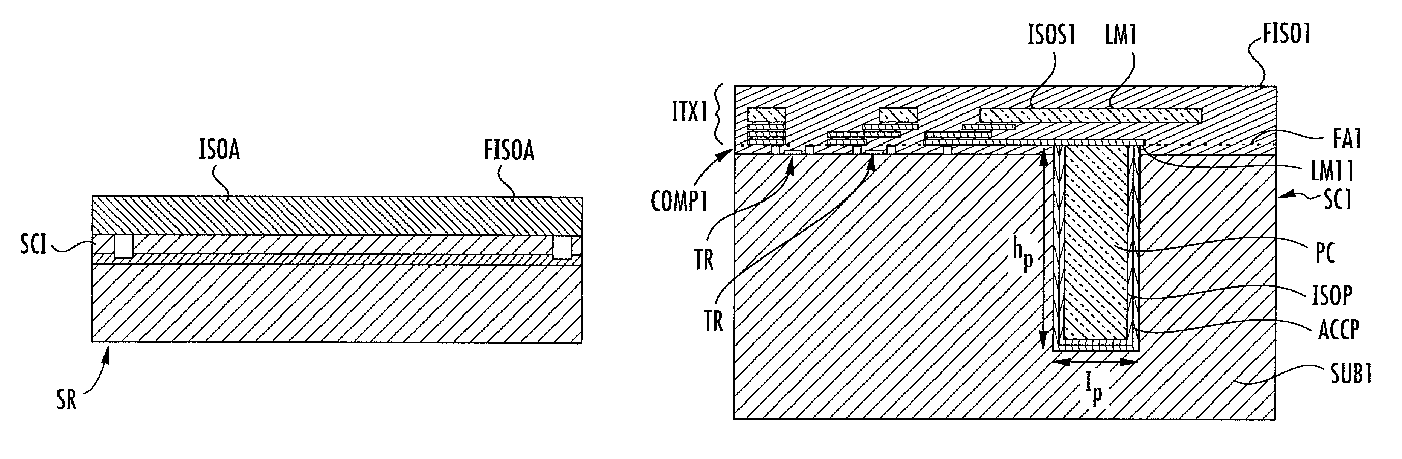
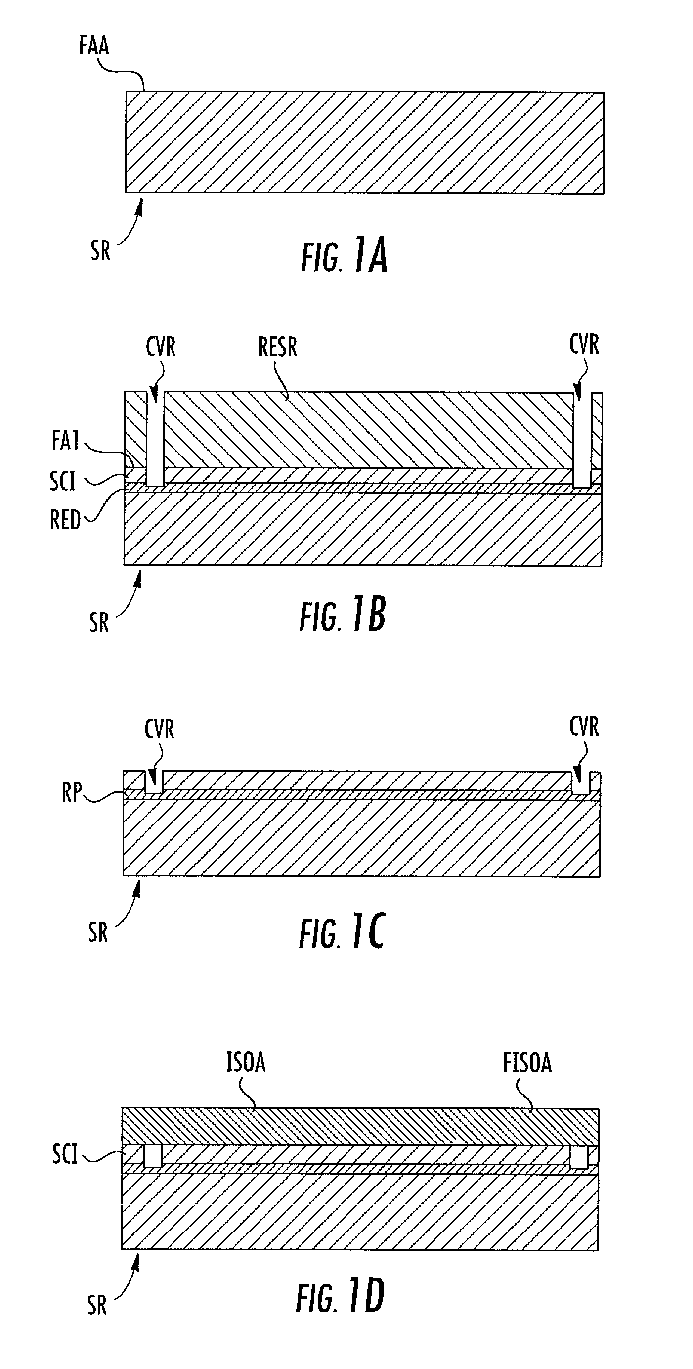
[0026]With reference to FIGS. 1A, 1B, 1C and 1D, the steps for fabrication of a handle within a rigid support SR will be described. The rigid support SR can, for example, be a semiconductor wafer comprising silicon, and its thickness can be on the order of several hundred micrometers, for example, 700 micrometers. Furthermore, a silicon wafer having a doping of the n type (producing an excess of electrons) can be used.

[0027]A step for implantation of atoms, for example, of boron, can be implemented from the face FAA of the support SR (FIG. 1B). The parameters of this implantation step (energy, temperature, duration, etc.) are chosen to obtain a buried doped region RED under an intermediate semiconductor layer SCI having a thickness of around 20 micrometers. Cavities CVR, here shown to be two in number, are then formed during a photolithographic step in which a photoresist RESR is opened up to form the cavities CVR which pass through the layer SCI and open into the buried doped regio...


PUM


Abstract

A method is for formation of an electrically conducting through-via within a first semiconductor support having a front face and comprising a silicon substrate. The method may include forming of a first insulating layer on top of the front face of the first semiconductor support, fabricating a handle including, within an additional rigid semiconductor support having an intermediate semiconductor layer, and forming on either side of the intermediate semiconductor layer of a porous region and of an additional insulating layer. The method may also include direct bonding of the first insulating layer and of the additional insulating layer, and thinning of the silicon substrate of the first semiconductor support so as to form a back face opposite to the front face.

Description

FIELD OF THE INVENTION[0001]The present disclosure relates to integrated circuits and, more particularly, to three-dimensional integrated structures comprising an assembly of at least two integrated circuits.BACKGROUND OF THE INVENTION[0002]Integrated circuits generally comprise, adjacent their front face, an interconnection network (BEOL: Back End Of Line) comprising metal lines. In order to form an electrical link between metal lines of two integrated circuits assembled front face against back face (or “back to front”), electrically conducting through-vias are formed, commonly denoted by the acronym TSV: Through Silicon Via. These links can be formed prior to the fabrication of the interconnection network of the integrated circuit, by forming a conducting pillar from the front face of the integrated circuit extending into the silicon substrate, then by thinning this substrate from its back face, the pillar then being exposed on the new back face. The electrically conducting throug...

Claims


Application Information

Patent Timeline
Patent Type & Authority Patents(United States)
IPC IPC(8): H01L21/66H01L21/762
CPCH01L24/81H01L21/6835H01L2225/06513H01L2224/9202H01L25/0657H01L2224/05548H01L2224/94H01L2224/81815H01L2224/81193H01L24/94H01L2224/17181H01L2224/11462H01L2924/01322H01L2224/16148H01L2221/68318H01L2224/81005H01L2221/68381H01L24/13H01L24/11H01L2221/68327H01L2225/06541H01L2224/13022H01L2224/02372H01L2221/6834H01L21/76898H01L2224/13082H01L2224/13147H01L2224/13024H01L2224/13111H01L2224/13009H01L2224/0401H01L2224/1147H01L2224/05569H01L2224/05008H01L2924/00014H01L2924/01047H01L2924/01029H01L2224/81H01L2224/11H01L2224/03H01L2924/00
Inventor CUZZOCREA, JULIENCHAPELON, LAURENT-LUC
Owner STMICROELECTRONICS (CROLLES 2) SAS
Why Eureka
Try Eureka