
Scan driver, light emitting display using the same, and driving method thereof

a technology of light-emitting display and scan driver, which is applied in the direction of electroluminescent light sources, static indicating devices, instruments, etc., can solve the problems of deteriorating aperture ratio, increasing power consumption of scan driver, and relatively heavy weight of crt display, so as to reduce the number of emission control lines, enhance the aperture ratio, and facilitate fabrication

Active Publication Date: 2014-03-18
SAMSUNG DISPLAY CO LTD
View PDF26 Cites 13 Cited by
  • Summary
  • Abstract
  • Description
  • Claims
  • Application Information

AI Technical Summary

Benefits of technology

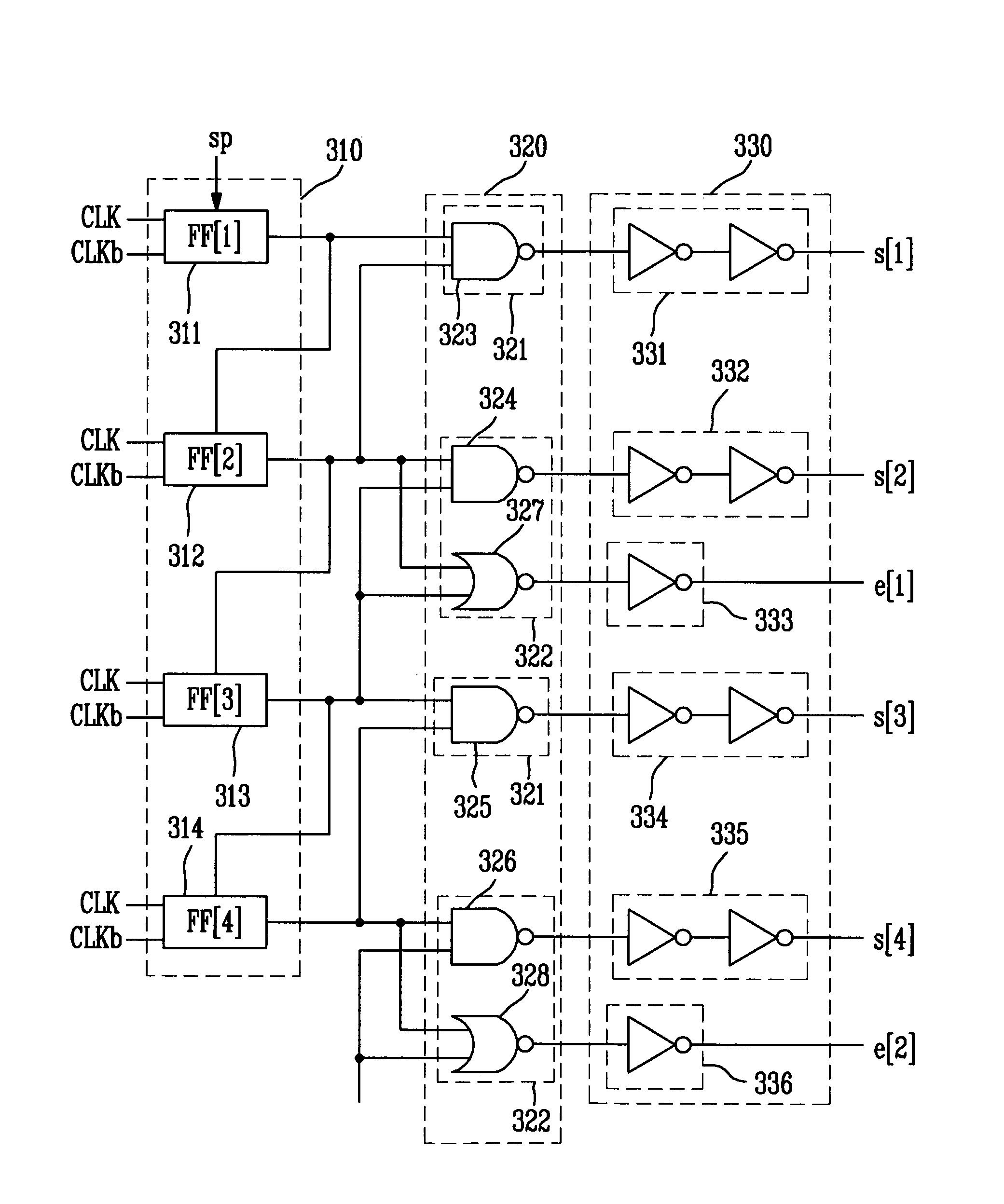
[0015]Accordingly, it is an aspect of the present invention to provide a scan driver, a light emitting display including the same, and a driving method thereof, in which the number of emission control lines is decreased to enhance an aperture ratio, and thus the number of signals outputted from the scan driver is also decreased, thereby making fabrication thereof easy and reducing power consumption.

Problems solved by technology

Recently, various flat panel displays have been developed to replace cathode ray tube (CRT) displays because the CRT displays are relatively heavy and bulky.
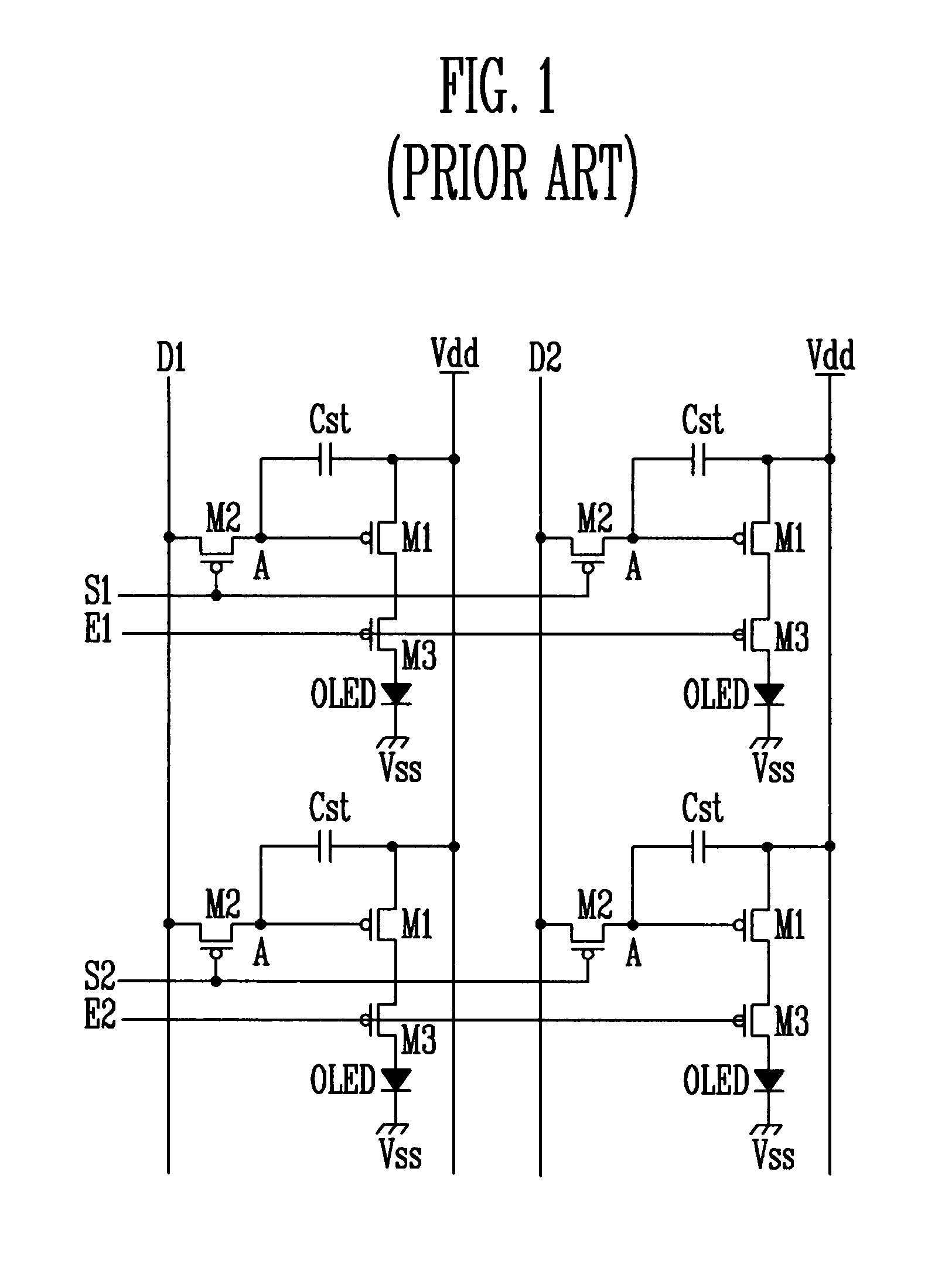
Therefore, the number of wiring lines is proportional to the number of emission control lines, thereby deteriorating an aperture ratio.
Therefore, the power consumption increases in the scan driver.
Further, the size of the scan driver is increased, thereby wastefully occupying much space of the light emitting display.

Method used


Image

  • Scan driver, light emitting display using the same, and driving method thereof
  • Scan driver, light emitting display using the same, and driving method thereof
  • Scan driver, light emitting display using the same, and driving method thereof

Examples


first embodiment

[0076]FIG. 10 is a circuit diagram of a current generator according to an exemplary embodiment of the present invention. By way of example, the current generator of FIG. 10 may be used as one or more of the current generators 115, 115′, 415 and 415′ of FIGS. 3, 5, 7 and 9. Referring to FIG. 10, the current generator includes a second transistor M22, a third transistor M23, and a capacitor Cst′. Here, each of the second transistor M22 and the third transistor M23 includes a gate, a source and a drain. Further, the capacitor Cst′ includes a first electrode and a second electrode.

[0077]The second transistor M22 includes the source connected to a power line Vdd, the drain connected to a first node N, and the gate connected to a second node A′. Here, the second node A′ is connected to the drain of the third transistor M23. The second transistor M22 supplies a current corresponding to the data signal to a light emitting device OLED.

[0078]The third transistor M23 includes the source connec...

second embodiment

[0089]FIG. 12 is a circuit diagram of a current generator according to an exemplary embodiment of the present invention. By way of example, the current generator of FIG. 10 may be used as one or more of the current generators 115, 115′, 415 and 415′ of FIGS. 3, 5, 7 and 9, respectively. Referring to FIG. 12, the current generator includes second through sixth transistors M32, M33, M34, M35 and M36, and a capacitor Cst″. Here, each of the second through sixth transistors M32 through M36 is a p-channel metal oxide semiconductor (PMOS) transistor, and includes a gate, a source and a drain. Further, the capacitor Cst″ includes a first electrode and a second electrode. In the described embodiment, there may not be any physical differences between each drain and each source of the second through sixth transistors M32 through M36. Alternatively, the source, the drain and the gate may be referred to as first, second and third electrodes, respectively.

[0090]The current generator of FIG. 12 i...


PUM


Abstract

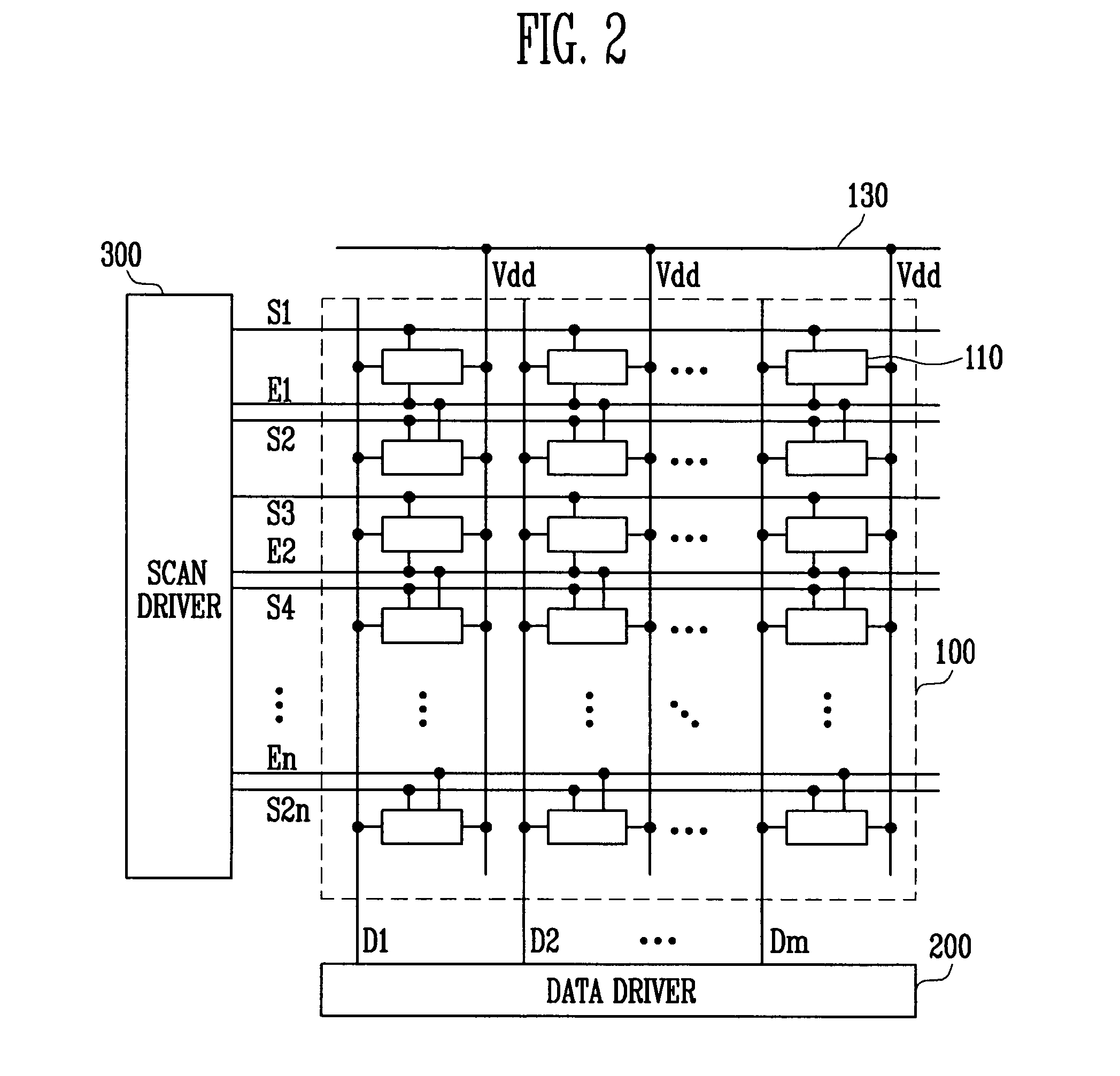
A light emitting display including: a plurality of scan lines adapted to transmit scan signals; a plurality of data lines adapted to transmit a data signal; a plurality of emission control lines adapted to transmit an emission control signal; and a plurality of pixels adapted to emit light in response to the scan signal, the data signal and the emission control signal. At least two pixels receiving the scan signals through different scan lines are connected to one emission control line. With this configuration, a scan driver and a light emitting display including the same have a decreased number of wiring lines provided in a pixel portion, thereby enhancing an aperture ratio, decreasing the number of emission control signals, decreasing the number of components and wiring lines needed for the scan driver, simplifying a fabrication process, and reducing the power consumption of the light emitting display.

Description

CROSS-REFERENCE TO RELATED APPLICATIONS[0001]This application claims priority to and the benefit of Korean Patent Application No. 10-2004-0086915, filed on Oct. 28, 2004, in the Korean Intellectual Property Office, the entire content of which is incorporated herein by reference.BACKGROUND[0002]1. Field of the Invention[0003]The present invention relates to a scan driver, a light emitting display including the same, a driving method thereof, and more particularly, to a scan driver, a light emitting display including the same, and a driving method thereof, in which the number of wiring lines is decreased, and the number of output lines connected to a scan driver is decreased, thereby enhancing an aperture ratio and reducing power consumption.[0004]2. Discussion of Related Art[0005]Recently, various flat panel displays have been developed to replace cathode ray tube (CRT) displays because the CRT displays are relatively heavy and bulky. Among the flat panel displays, a light emitting d...

Claims


Application Information

Patent Timeline
Patent Type & Authority Patents(United States)
IPC IPC(8): G09G3/30H05B44/00
CPCG09G3/3233G09G2300/0861G09G2320/043G09G2300/0842G09G2300/0819G09G2300/0465G09G3/3266G09G3/30
Inventor EOM, KI MYEONGOH, CHOON YUL
Owner SAMSUNG DISPLAY CO LTD
Learn More