
Sensor for semiconductor degradation monitoring and modeling

a technology of degradation monitoring and modeling, applied in the field of sensor technology, can solve the problems of limited life span of semiconductors, gradual or abrupt failure of semiconductor systems, and limited advancement in semiconductor technology, and achieve the effect of reducing the degredation of semiconductor systems

Active Publication Date: 2014-03-25
SDEP CORP
View PDF15 Cites 2 Cited by
  • Summary
  • Abstract
  • Description
  • Claims
  • Application Information

AI Technical Summary

Benefits of technology

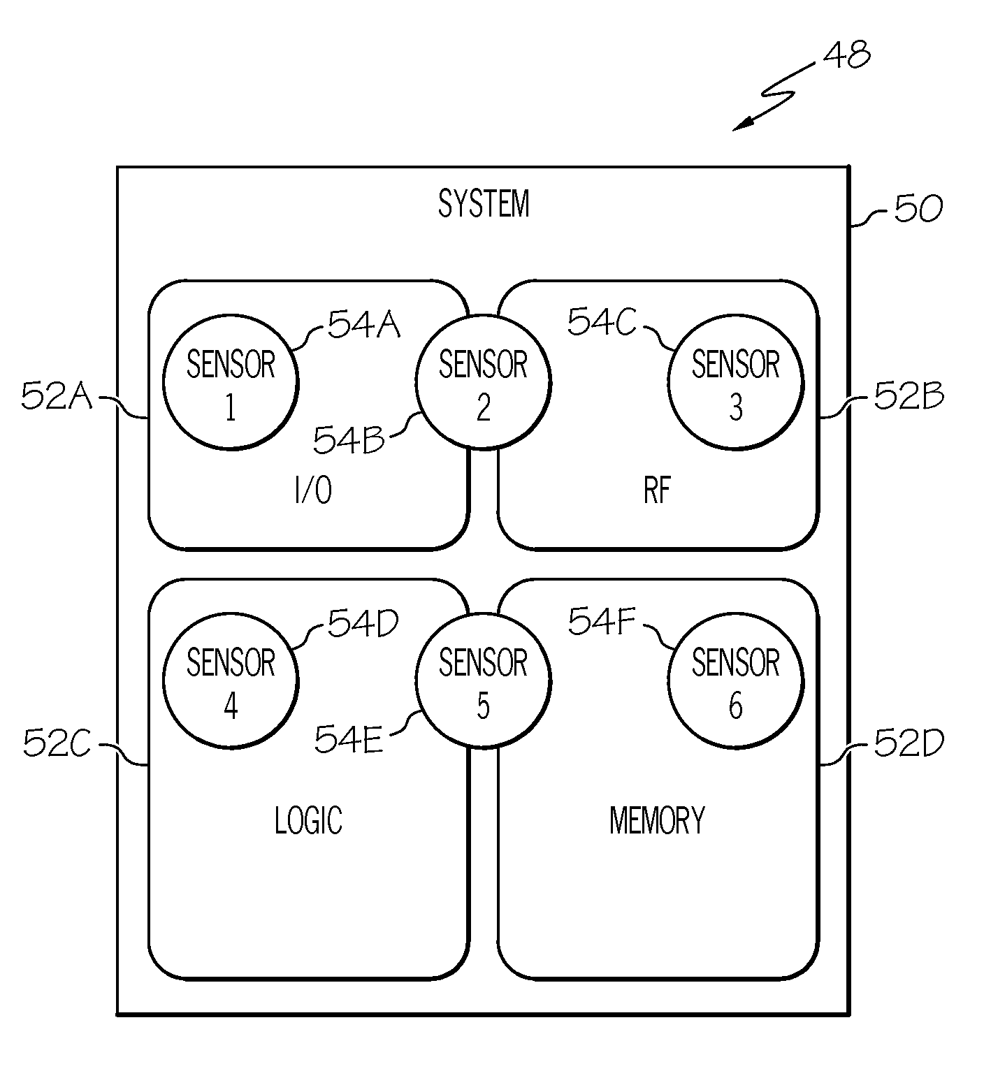
The present invention provides a system and method for improving the reliability of semiconductor sensors by positioning them in critical locations within the system. The sensors are designed to have maximum sensitivity to process variations and are connected as a network, with each sensor representing a behavior of its location. The sensors have mode selection and operational trigger inputs that allow them to have an operational mode for aging and a measurement mode for outputting the age of the sensors. This information is used to modify one or more functional blocks in real-time to reduce semiconductor system degredation.

Problems solved by technology

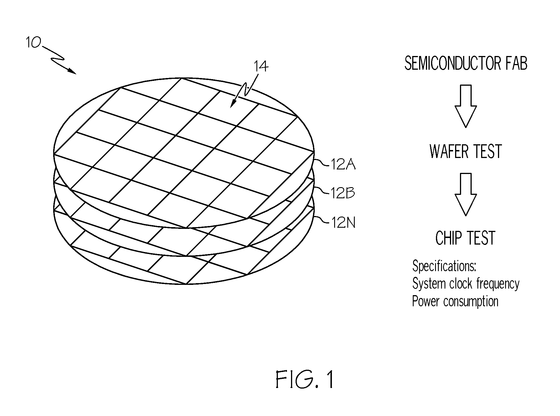
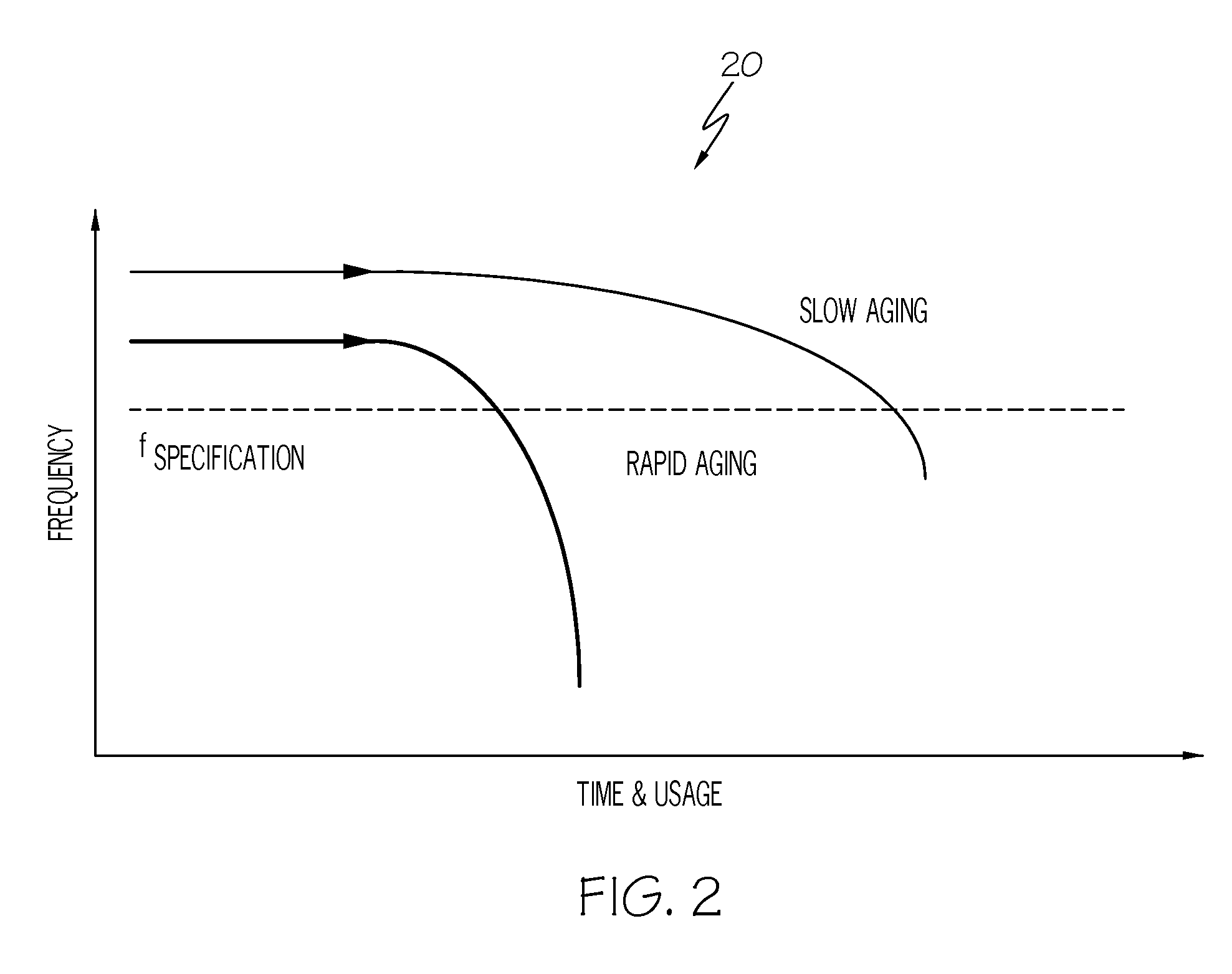
Advancement in semiconductor technology is often limited by semiconductors' limited life span.
Specifically, a semiconductor system suffers from gradual or abrupt failures due to aging.
Along these lines, accumulated quantum mechanical effects cause semiconductor device failure even under nominal operation conditions.
Such failure dramatically degrades system performance and reliability.
Such an approach, however, is not useful to measure individual chip aging since: it does not experience circuit switching behaviors; it does not imitate system operation pattern in practice; and it requires high precision data converters.
However, none of these previous attempts provide an accurate way to truly model the age of semiconductors and / or functional blocks thereof.

Method used


Image

  • Sensor for semiconductor degradation monitoring and modeling
  • Sensor for semiconductor degradation monitoring and modeling
  • Sensor for semiconductor degradation monitoring and modeling

Examples


Embodiment Construction

[0036]Illustrative embodiments now will be described more fully herein with reference to the accompanying drawings, in which exemplary embodiments are shown. This disclosure may, however, be embodied in many different forms and should not be construed as limited to the exemplary embodiments set forth herein. Rather, these exemplary embodiments are provided so that this disclosure will be thorough and complete and will fully convey the scope of this disclosure to those skilled in the art. In the description, details of well-known features and techniques may be omitted to avoid unnecessarily obscuring the presented embodiments.

[0037]The terminology used herein is for the purpose of describing particular embodiments only and is not intended to be limiting of this disclosure. As used herein, the singular forms “a”, “an”, and “the” are intended to include the plural forms as well, unless the context clearly indicates otherwise. Furthermore, the use of the terms “a”, “an”, etc., do not de...


PUM


Abstract

The present invention provides in-situ positioning of a sensor within each functional block, as well as at critical locations, of a semiconductor system. Sensor quantity and location is optimized for maximum sensitivity to known process variations. The sensor models a behavior of the location in which it is positioned and comprises a plurality of stages connected as a network and a self-digitizer. Each sensor has a mode selection input for selecting a mode thereof and an operational trigger input for enabling the sensor to model the behavior. The model selection input and operation trigger enable the sensor to have an operational mode in which the plurality of sensors are subject to an aging process, as well as a measurement mode in which an age of the plurality of sensors is outputted. Based on the output, one or more functional blocks are modified to reduce semiconductor system gradation in real-time.

Description

TECHNICAL FIELD[0001]The present invention relates to sensor technology. Specifically, the present invention relates to a reliability sensor timing method, and the in-situ positioning / assimilation of reliability sensors within functional blocks and critical locations of a semiconductor system.BACKGROUND OF THE INVENTION[0002]Advancement in semiconductor technology is often limited by semiconductors' limited life span. Specifically, a semiconductor system suffers from gradual or abrupt failures due to aging. Along these lines, accumulated quantum mechanical effects cause semiconductor device failure even under nominal operation conditions. Such failure dramatically degrades system performance and reliability. Previous approaches provide estimated life span only. That is, previous approaches attempt to predict the reliability of device technology and publish it as a specification. Such an approach, however, is not useful to measure individual chip aging since: it does not experience c...

Claims


Application Information

Patent Timeline
Patent Type & Authority Patents(United States)
IPC IPC(8): H01L23/58H01L21/66
CPCG01R31/2856H01L23/58H01L22/34H01L2924/0002H01L2924/00
Inventor KIM, MOON, J.
Owner SDEP CORP
Learn More