Orientation of an electronic CMOS structure with respect to a buried structure in the case of a bonded and thinned-back stack of semiconductor wafers

a technology of electronic cmos and buried structures, which is applied in the direction of electrical appliances, basic electric elements, instruments, etc., can solve problems such as the recess or withdrawal of the perimeter or edg

Active Publication Date: 2014-04-08
X FAB SEMICON FOUNDRIES
View PDF14 Cites 1 Cited by
  • Summary
  • Abstract
  • Description
  • Claims
  • Application Information

AI Technical Summary

Benefits of technology

[0011]It is an object of the present invention to provide a method of the above-identified type such that the indicated disadvantages may be avoided, in particular an alignment of “front side to rear side” is to be avoided or the necessity of providing rear side alignment marks is to be avoided, while nevertheless an alignment of marks for the front side should be possible.
[0023]The embodiments of the invention are advantageous in that the alignment of the front side with respect to the rear side is not necessary, thereby resulting in increased alignment accuracy and thus in increased yield and quality improvement.
[0024]A further advantage is the fact that a rear side processing for producing rear side alignment marks is not necessary, thereby reducing the processing efforts and the risk of damaging the front side (the bonding side).
[0025]Since the alignment marks are provided at the edge of the wafer advantageously a significantly higher robustness of the assembly is achieved with respect to offset and rotation and also a significantly reduced patterning complexity is achieved, in particular by the withdrawal or recessing of the wafer edge. The claimed invention also avoids patterning-related issues of the type as mentioned above.
[0027]The circumference of the cover wafer may also be uniformly thinned which advantageously reduces the probability of stress during the fabrication and handling of the structure.
[0028]A further advantageous embodiment of the inventive method is characterized in that the edge of each thinned part of the thinned portion of the cover wafer provided from the bond side has sections of linear edges. In this manner, the alignment of the wafer stack with respect to the masks of the at least one circuit structure to be implemented may be simplified.

Problems solved by technology

This “edge modification” results in a withdrawal or recess of the perimeter or edge.

Method used


Image

  • Orientation of an electronic CMOS structure with respect to a buried structure in the case of a bonded and thinned-back stack of semiconductor wafers
  • Orientation of an electronic CMOS structure with respect to a buried structure in the case of a bonded and thinned-back stack of semiconductor wafers
  • Orientation of an electronic CMOS structure with respect to a buried structure in the case of a bonded and thinned-back stack of semiconductor wafers

Examples


Embodiment Construction

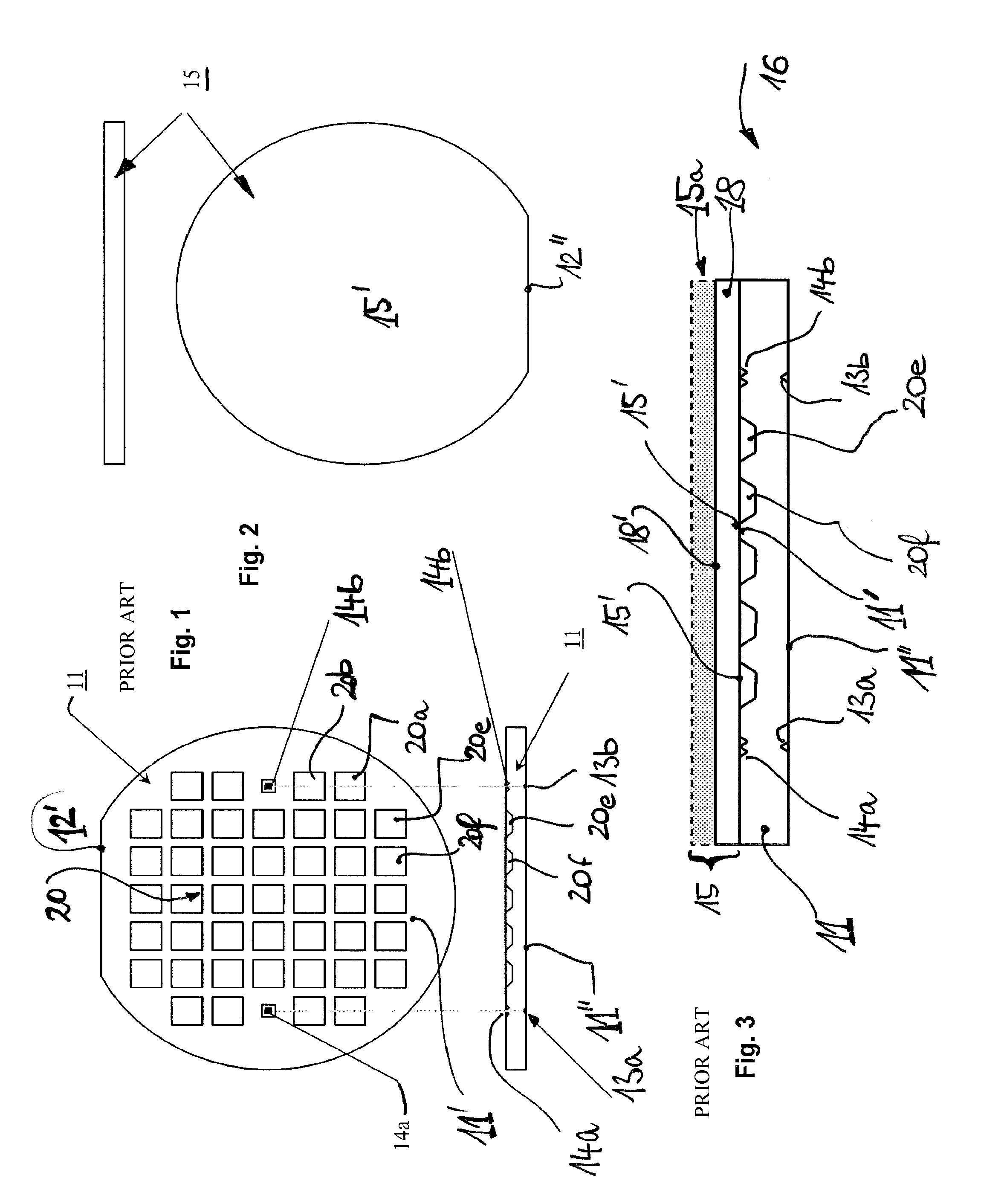
[0041]FIGS. 1 to 3 illustrate the approach corresponding to the prior art. The situation on the bond surface 11′ of the cavity wafer 11 is illustrated in FIG. 1 as a top view. In this case, the structure 20 consisting of depressions 20a, 20b, 20e and others to be etched into the wafer surface are visible.

[0042]Alignment marks 14a, 14b are clearly spaced apart from the wafer edge and are positioned in the vicinity of the edge structure 20. The sectional view of FIG. 1 illustrates alignment marks 13a, 13b on the rear side 11′ of the cavity wafer 11, which correspond to the alignment marks 14a, 14b.

[0043]Reference signs 12′ and 12″ indicate a main flattening as a linear edge for both the wafer 11 and the wafer 15.

[0044]In FIG. 2 there is shown the non-processed cover wafer 15 used for covering the cavity wafer 11. The surface to be bonded is 15′. Wafers 11 and 15 are bonded. The bonded wafer stack 16 is formed. The stack is shown in FIG. 3 in sectional view—after thinning 15a of the c...


PUM


Abstract

A method for aligning an electronic CMOS structure with respect to a buried structure in the case of a bonded and thinned back stack of semiconductor wafers. The method for aligning the electronic CMOS structure may include forming alignment marks in the process of fabricating the structure to be buried on a front side, which is used for bonding of the semiconductor wafer, which includes the structure to be buried. The alignment marks may be formed on the edge of the semiconductor wafer. The method for aligning the electronic CMOS structure may include providing a cover wafer with first thinned portions of the wafer thickness provided from the bonding side at positions corresponding to positions of the alignment marks. After the thinning of the cover wafer a plan view of the alignment mark is obtained after the wafer bonding that initially results in a burying of the structures, wherein subsequently the resulting wafer stack is thinned to a certain degree with respect to the cover wafer, thereby making visible the at least one alignment mark, and by means of the alignment mark masks of method steps for fabricating the electronic structure on the surface of the thinned cover wafer are aligned.

Description

CROSS-REFERENCE TO RELATED APPLICATIONS[0001]The application is a U.S. National Stage Application of International Application of PCT / IB2009 / 053268 filed Jul. 27, 2009, which claims the benefit of German Patent Application No. 10 2008 035 055.9 filed Jul. 26, 2008, the disclosures of which are herein incorporated by reference in their entireties.FIELD OF THE DISCLOSURE[0002]The invention is based on a method for orienting or aligning of an electronic CMOS structure with respect to a buried structure for a bonded and thinned-back stack of semiconductor wafers.[0003]In the process of fabricating the structures to be buried on the front side of the semiconductor wafer, which is used for the bonding process and which bears the structure to be buried, alignment marks are formed. Bonding of a cover wafer is accomplished by thinning the wafer thickness from the bonding side at locations that correspond in their positions to the alignment marks such that visibility as a top view of the alig...

Claims


Application Information

Patent Timeline
Patent Type & Authority Patents(United States)
IPC IPC(8): H01L21/76
CPCH01L2223/54493H01L23/544G01L9/0042H01L2223/54426H01L2223/54466H01L2924/0002H01L2924/00
Inventor KLINGNER, HOLGERUNGELENK, JENS
Owner X FAB SEMICON FOUNDRIES
Why Eureka
Try Eureka