Semiconductor package and fabrication method thereof

a technology of semiconductor chips and semiconductor chips, applied in the direction of semiconductor/solid-state device details, semiconductor devices, electrical apparatus, etc., can solve the problems of reducing the structural adversely affecting the product quality, and reducing the surface strength of the semiconductor chip, so as to enhance the bonding and reinforce the bonding

Inactive Publication Date: 2014-04-15
SILICONWARE PRECISION IND CO LTD
View PDF13 Cites 4 Cited by
  • Summary
  • Abstract
  • Description
  • Claims
  • Application Information

AI Technical Summary

Benefits of technology

[0009]Another objective of the present invention is to provide a semiconductor package and a fabrication method thereof, for preventing delamination on the corners of a semiconductor chip in the semiconductor package.
[0010]Still another objective of the present invention is to provide a semiconductor package and a fabrication method thereof, for preventing cracks of a semiconductor chip caused by roughening the semiconductor chip.
[0011]A further objective of the present invention is to provide a semiconductor package and a fabrication method thereof, for maintaining the structural strength of a roughened semiconductor chip.
[0014]The roughened structure on the peripheral portion of the non-active surface of the semiconductor chip is primarily formed at the corners of the semiconductor chip. The roughened structure extends for at least one third of a distance from the corner of the semiconductor chip to a center of the non-active surface of the semiconductor chip, that is, one third of a distance to neutral point (DNP). The roughened structure formed on the non-active surface of the semiconductor chip reinforces the bonding between the semiconductor chip and the encapsulant. The non-roughened central portion of the non-active surface of the semiconductor chip maintains the structural strength of the semiconductor chip.
[0015]Therefore, according to the semiconductor package and the fabrication method thereof in the present invention, the peripheral portion of the non-active surface of the semiconductor chip is roughened to form the roughened structure, for example, at the corners of the semiconductor chip. The roughened structure extends for at least one third of the distance to neutral point (DNP), and enhances the bonding between the semiconductor chip and the encapsulant. The non-roughened central portion of the non-active surface of the semiconductor chip maintains the structural strength of the semiconductor chip. Accordingly, the present invention is suitable for packaging a large semiconductor chip, without having delamination on the corners of the semiconductor chip, and without having cracks of the semiconductor chip caused by roughening the entire chip surface in the prior art.

Problems solved by technology

As a result, delamination usually occurs at the corners of the semiconductor chip and adversely affects the product quality.
However, roughening the surface of the semiconductor chip decreases the surface strength of the semiconductor chip.
For a semiconductor chip to be used in a compact package for a miniaturized electronic product, the semiconductor chip must be thinned, and roughening a non-active surface of such thinned semiconductor chip would greatly reduce the structural strength of the semiconductor chip and thereby lead to cracks of the semiconductor chip.
This situation becomes more severe for a thin and large semiconductor chip.

Method used


Image

  • Semiconductor package and fabrication method thereof
  • Semiconductor package and fabrication method thereof
  • Semiconductor package and fabrication method thereof

Examples


Embodiment Construction

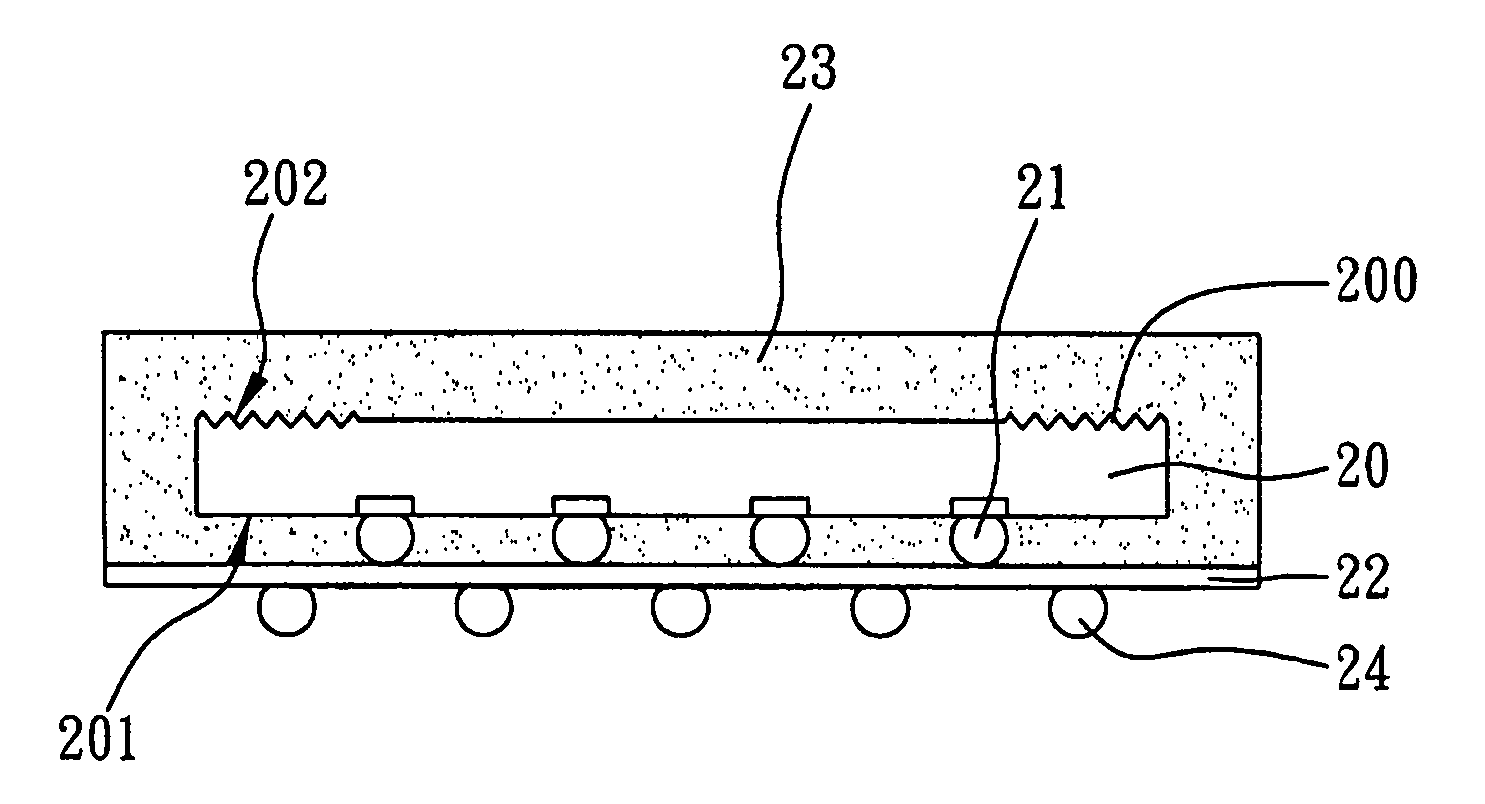
[0020]Preferred embodiments of a semiconductor packages and a fabrication method thereof as proposed in the present invention are described as follows with reference to FIGS. 2 to 5. It should be understood that the drawings are simplified schematic diagrams only showing the elements relevant to the present invention, and the layout of elements could be more complicated in practical implementation.

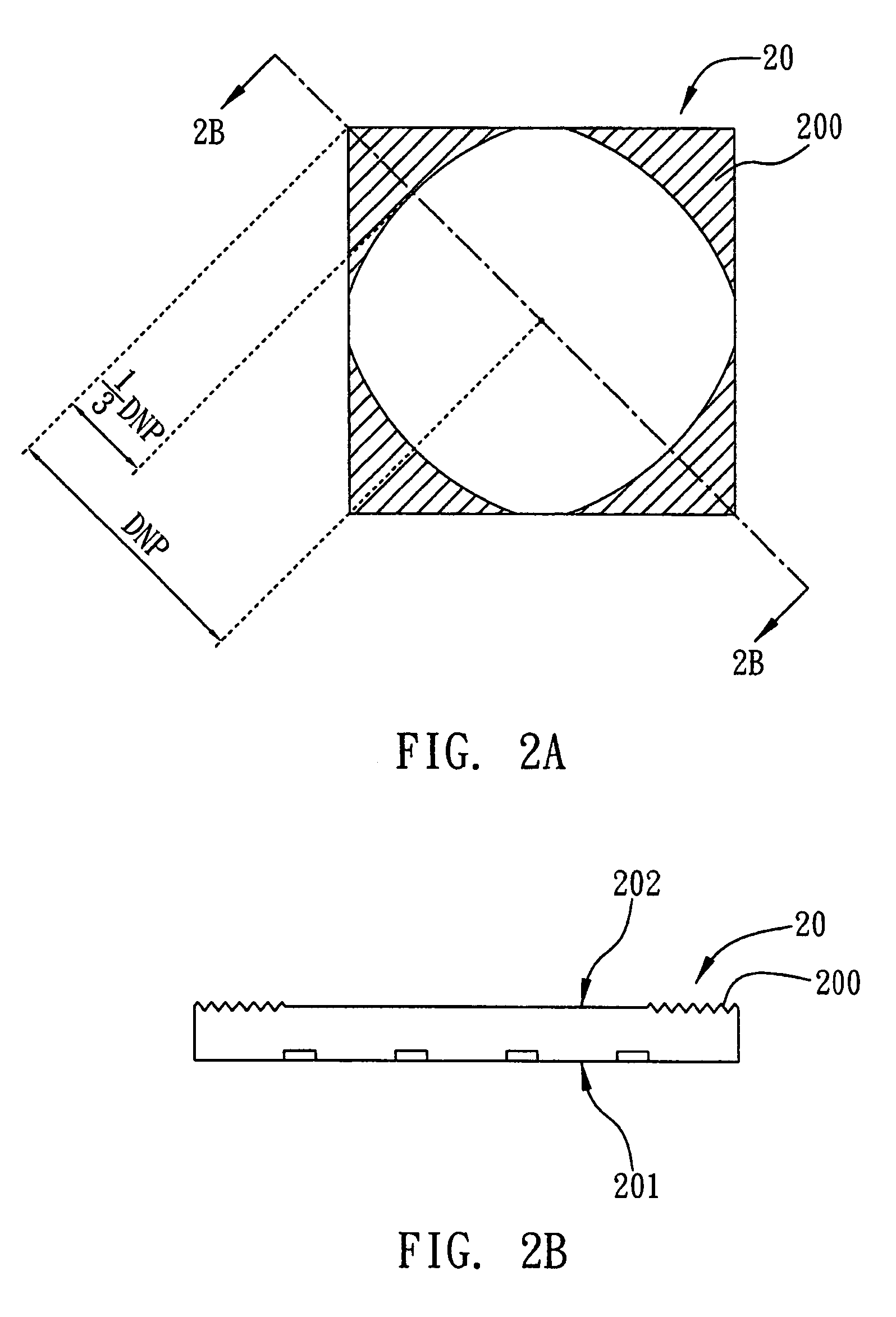
[0021]FIGS. 2A to 2C show a semiconductor package and a fabrication method thereof in accordance with the present invention.

[0022]As shown in FIGS. 2A and 2B, wherein FIG. 2B is a cross-sectional view of FIG. 2A taken along line 2B-2B, a semiconductor package of the present invention comprises a semiconductor chip 20. The semiconductor chip 20 has an active surface 201 and a non-active surface 202 opposing to the active surface 201. A roughened structure 200 is formed on a peripheral portion of the non-active surface 202 of the semiconductor chip 20, such that the non-active surface 202 is...


PUM


Abstract

A semiconductor package and a fabrication method thereof are disclosed. The fabrication method includes the steps of providing a semiconductor chip having an active surface and a non-active surface opposing to the active surface, roughening a peripheral portion of the non-active surface so as to divide the non-active surface into the peripheral portion formed with a roughened structure and a non-roughened central portion, mounting the semiconductor chip on a chip carrier via a plurality of solder bumps formed on the active surface, forming an encapsulant on the chip carrier to encapsulate the semiconductor chip. The roughened structure formed on the peripheral portion of the non-active surface of the semiconductor chip can reinforce the bonding between the semiconductor chip and the encapsulant, and the non-roughened central portion of the non-active surface of the semiconductor chip can maintain the structural strength of the semiconductor chip.

Description

FIELD OF THE INVENTION[0001]The present invention relates to semiconductor packages and fabrication methods thereof, and more particularly, to a flip-chip semiconductor package and a fabrication method thereof.BACKGROUND OF THE INVENTION[0002]A molded flip-chip semiconductor package is comprised of a semiconductor chip electrically connected to a surface of a substrate via a plurality of solder bumps mounted on an active surface of the semiconductor chip, an encapsulant formed on the surface of the substrate by a molding process to encapsulate the semiconductor chip, and a plurality of solder balls implanted on an opposite surface of the substrate and serving as I / O terminals for electrically connecting the semiconductor chip to an external device. Such package design greatly reduces the size of the package, such that the semiconductor chip and the substrate can be made comparable in size. The flip-chip design also eliminates the use of conventional bonding wires, thereby desirably ...

Claims


Application Information

Patent Timeline
Patent Type & Authority Patents(United States)
IPC IPC(8): H01L23/48H01L23/28
CPCH01L2924/3011H01L23/3142H01L21/561H01L2224/16225H01L29/0657H01L23/3128H01L2924/15311H01L2924/10158H01L2224/0557H01L2224/05573H01L2924/00014H01L2224/05571H01L2224/0554H01L2224/05599H01L2224/0555H01L2224/0556
Inventor HUANG, WEN-HOMETSENG, WEN-TSUNGLIN, CHANG-FUTSAI, HO-YIHSIAO, CHENG-HSU
Owner SILICONWARE PRECISION IND CO LTD
Why Eureka
Try Eureka