
High voltage fast recovery trench diode

a diode and trench technology, applied in the field of high-voltage trench diodes, can solve the problems of increasing the leakage current in the diode, reducing the injection efficiency, and increasing the voltage across the devi

Active Publication Date: 2014-04-29
ALPHA & OMEGA SEMICON INC
View PDF6 Cites 14 Cited by
  • Summary
  • Abstract
  • Description
  • Claims
  • Application Information

AI Technical Summary

Benefits of technology

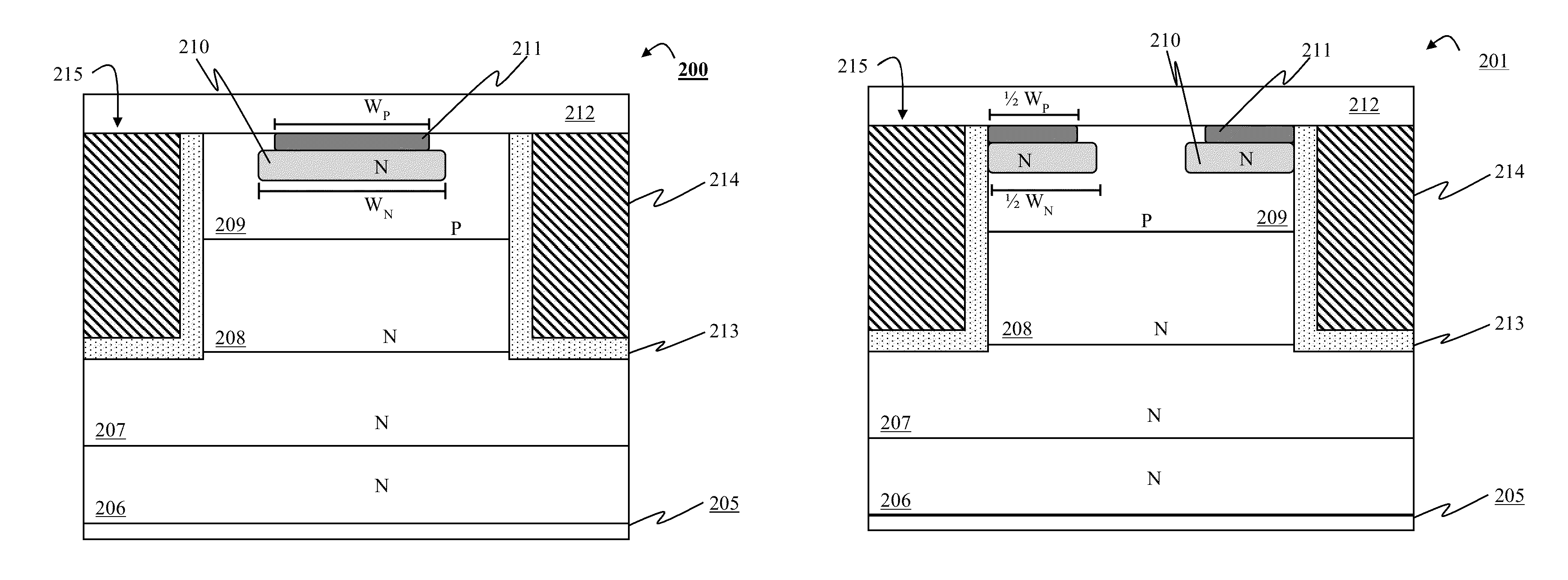
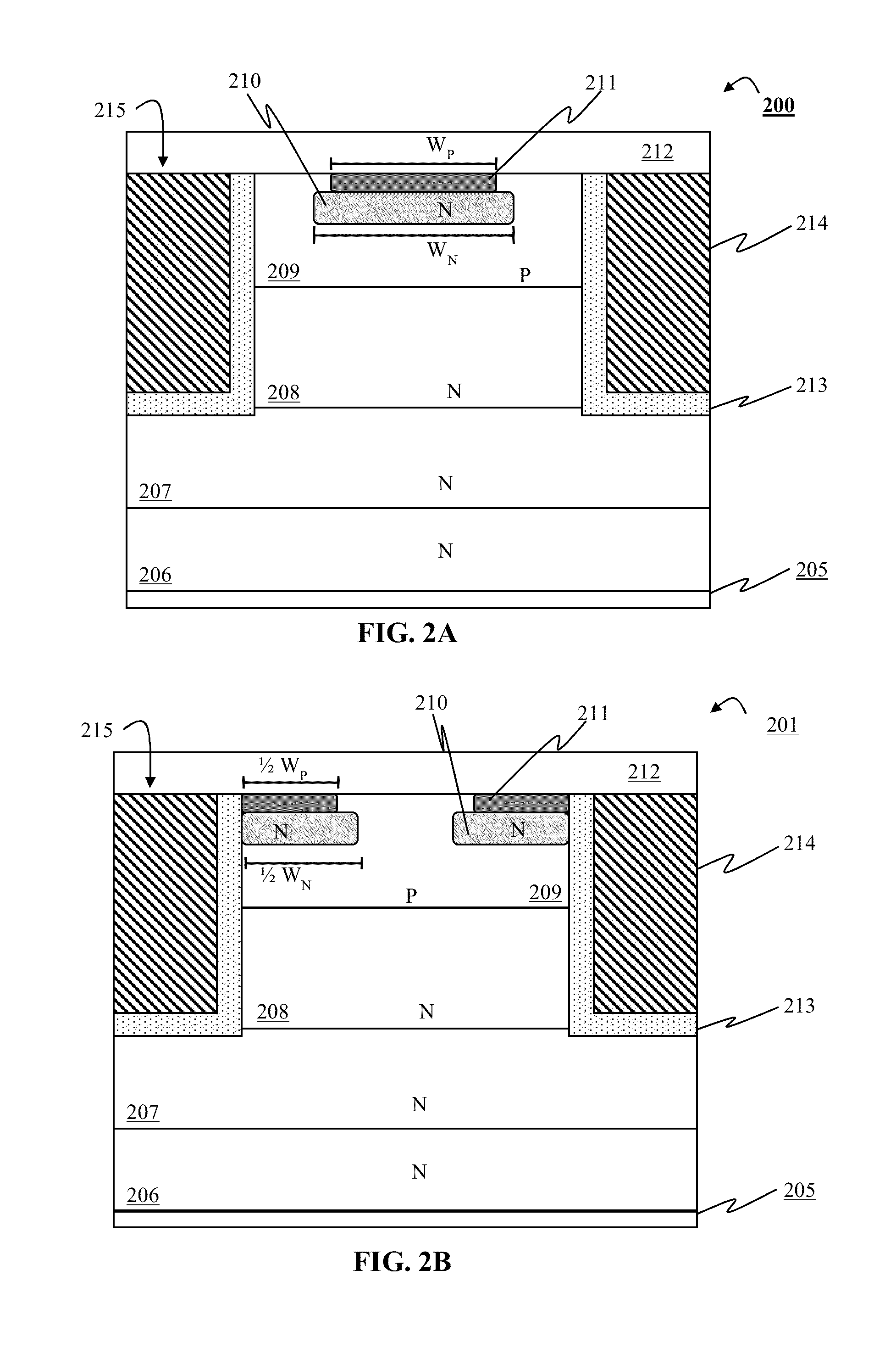
This patent is about improving the performance of high voltage trench based diodes by reducing the injection efficiency and stray circuit inductance. The invention proposes a method to decrease the reverse recovery time of a diode by reducing the value of Qrr (the charge that needs to be removed during the reverse recovery period). This is done by decreasing both the value of Irm (the reverse recovery current) and the concentration of holes in the device. The invention also discusses alternative techniques for reducing injection efficiency, such as doping the top P-layer and removing the semiconductor substrate. The invention proposes a trench diode with N and P-pockets to further enhance the performance of the diode. The technical effects of the invention include reducing the reverse recovery time of a diode and improving its performance.

Problems solved by technology

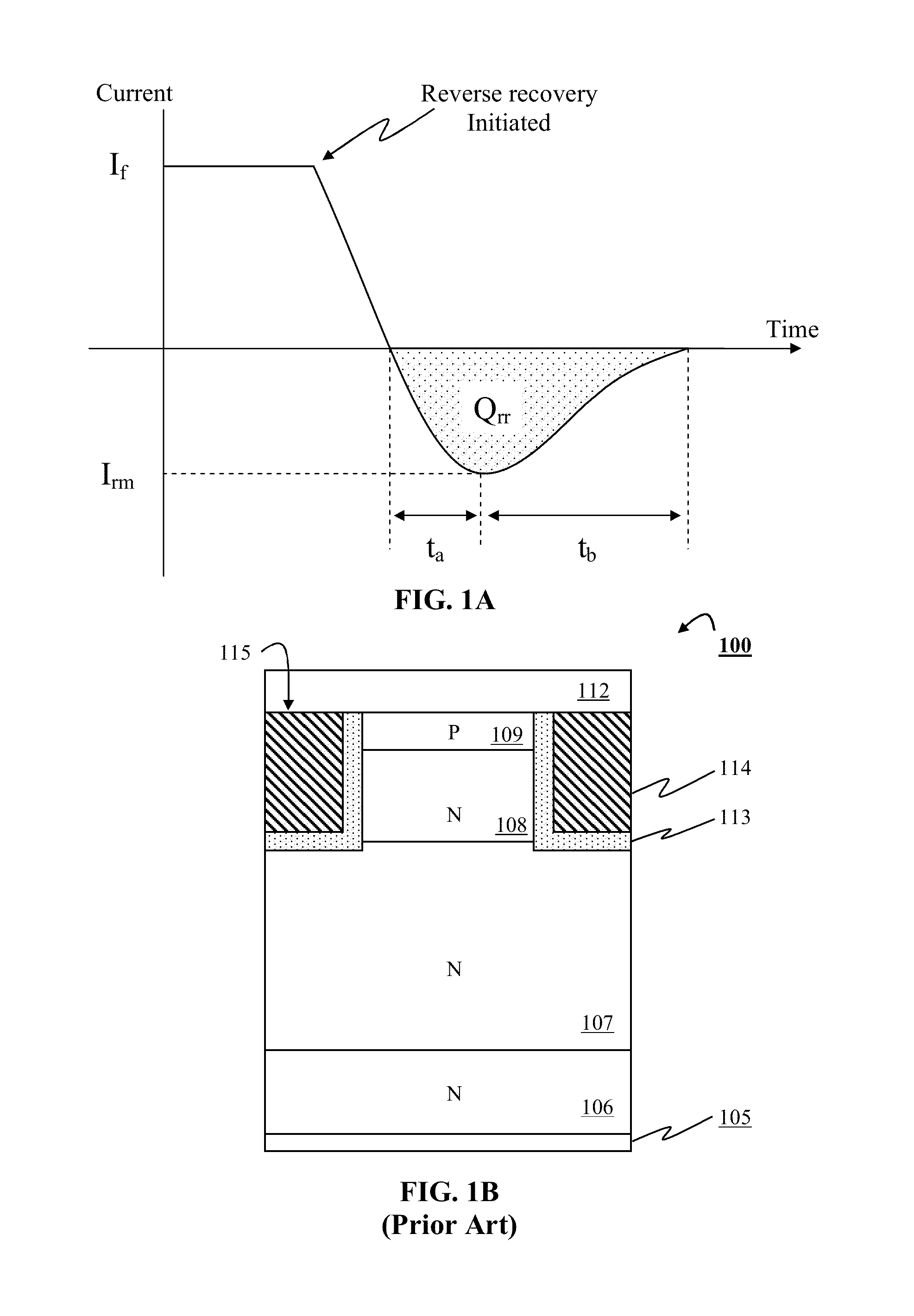
However, if the reverse current falls too sharply towards the end of the reverse recovery period, stray circuit inductance may cause an increased voltage across the device.
Prior art attempts to reduce the Qrr have therefore focused on reducing the injection efficiency.
However, these processes also lead to increased leakage current in the diode and degraded reverse recovery performance at high temperature.
The light doping reduces the injection efficiency from the top side of the device because there are fewer charge carriers available.

Method used


Image

  • High voltage fast recovery trench diode
  • High voltage fast recovery trench diode
  • High voltage fast recovery trench diode

Examples


Embodiment Construction

[0017]Although the following detailed description contains many specific details for the purposes of illustration, anyone of ordinary skill in the art will appreciate that many variations and alterations to the following details are within the scope of the invention. Accordingly, the exemplary embodiments of the invention described below are set forth without any loss of generality to, and without imposing limitations upon, the claimed invention. In the following discussion, devices with an N-type epitaxial layer and a P-type top layer are described for purposes of illustration. Substantially similar devices may be fabricated using a similar process but with opposite conductivity types.

[0018]Aspects of the present disclosure describe high voltage fast recovery trench diodes and methods for making the same. The device may have trenches that extend at least through a top P-layer and an N-barrier layer. The N-barrier layer may have a higher doping concentration than the N-drift layer. ...


PUM


Abstract

Aspects of the present disclosure describe high voltage fast recovery trench diodes and methods for make the same. The device may have trenches that extend at least through a top P-layer and an N-barrier layer. A conductive material may be disposed in the trenches with a dielectric material lining the trenches between the conductive material and sidewalls of the trenches. A highly doped P-pocket may be formed in an upper portion of the top P-layer between the trenches. A floating N-pocket may be formed directly underneath the P-pocket. The floating N-pocket may be as wide as or wider than the P-pocket. It is emphasized that this abstract is provided to comply with rules requiring an abstract that will allow a searcher or other reader to quickly ascertain the subject matter of the technical disclosure. It is submitted with the understanding that it will not be used to interpret or limit the scope or meaning of the claims.

Description

FIELD OF THE INVENTION[0001]This invention generally relates to semiconductor diodes. Specifically, the invention is directed to high voltage trench based diodes.BACKGROUND OF THE INVENTION[0002]The reverse recovery behavior of a diode is shown in the graph presented in FIG. 1A. Initially, the diode is conducting current in the forward direction. Once the reverse recovery is initiated, the forward current begins to decrease, and ultimately begins flowing in the reverse direction. The reverse current increases during the time ta until it reaches the maximum reverse recovery current Irm. Thereafter, during the period of time tb the reverse current decreases until it returns to approximately zero. At this point the diode is able to block the reverse flow of current. The reverse current flow during ta and tb allows the diode to remove the charge that has built up in the device while it is turned on in the forward state. The total amount of charge that needs to be removed (the reverse re...

Claims


Application Information

Patent Timeline
IPC IPC(8): H01L29/66
CPCH01L29/66136H01L29/0615H01L29/861H01L29/0692H01L21/02104H01L29/36H01L29/66H01L29/8613
Inventor HU, JUNPADMANABHAN, KARTHIKBOBDE, MADHURYILMAZ, HAMZA
Owner ALPHA & OMEGA SEMICON INC
Learn More