Method for forming silicon-containing dielectric film by cyclic deposition with side wall coverage control

a dielectric film and cyclic deposition technology, applied in chemical vapor deposition coating, coating, metallic material coating process, etc., can solve the problems of thin deterioration of film deposited on a sidewall, and low sidewall reaction rate of nitration

Active Publication Date: 2014-05-13
ASM IP HLDG BV
View PDF8 Cites 407 Cited by
  • Summary
  • Abstract
  • Description
  • Claims
  • Application Information

AI Technical Summary

Problems solved by technology

This problem may be caused by ion collision interfering with reaction speed on the sidewall as compared with that on a top or bottom surface.
Particularly, nitration has a low rate of sidewall reaction as compared with oxidation, causing problems of thin film deposited on a sidewall, deterioration of film deposited on a sidewall, etc.

Method used


Image

  • Method for forming silicon-containing dielectric film by cyclic deposition with side wall coverage control
  • Method for forming silicon-containing dielectric film by cyclic deposition with side wall coverage control
  • Method for forming silicon-containing dielectric film by cyclic deposition with side wall coverage control

Examples


example 8

[0130]Precursor: Tetrachlorodimethylsilane

[0131]Precursor inflow pressure: 66.6 Pa

[0132]Substrate temperature: 400° C.

[0133]Carrier gas flow: Ar at 2 SLM

[0134]Reactant gas flow: H2 at 0.5 SLM

[0135]RF frequency: 13.56 MHz

[0136]RF power: 400 W

[0137]Precursor supply time (steps 1a+2a): 2 seconds

[0138]RF Plasma exciting time (step 2a): 1.3 seconds

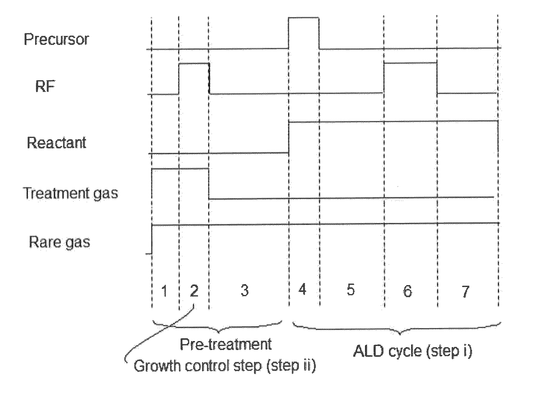
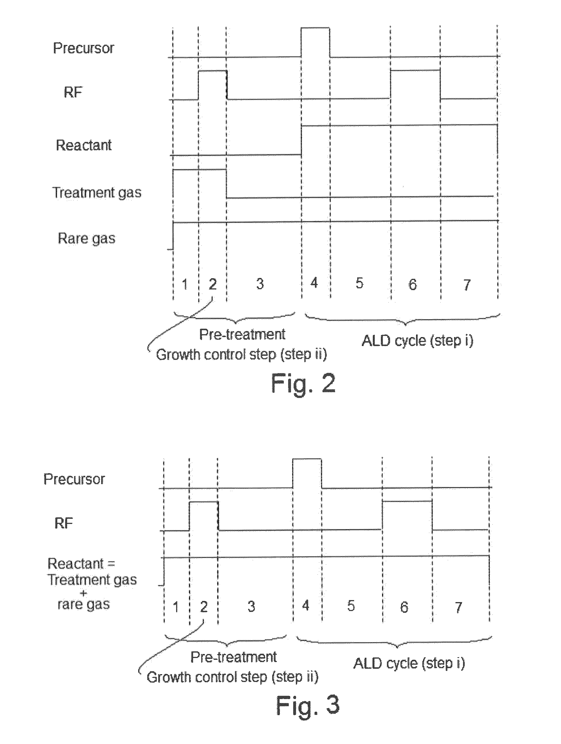
[0139]The growth control step (step 2 in FIG. 2; step 3a in FIG. 5) was performed under conditions shown in Table 1. Incidentally, the duration of step 1 in FIG. 2 was 0.5 seconds, and the duration of step 3 in FIG. 2 was 0.5 seconds.

[0140]

TABLE 1CyclesperTotalgrowthdepositionTem.TreatmentRareRFDurationPressurecontrolcyclesFilm(° C.)gasgas(W)(sec)(Pa)(N)(M · N)Com 1SiN400500Ex 1SiN400H2:He:500604005005001SLM1SLMEx 2SiN400H2:He:5000.140015001SLM1SLMCom 2SiC400500Ex 3SiC100H2:He:500603005005000.5SLM1SLMEx 4SiC100H2:He:5000.230015000.5SLM1SLMEx 5SiC400NH3:He:400604005005001SLM1SLMEx 6SiC400NH3:He:4000.140015001SLM1SLMEx 7SiC400CH4He:40060400500500...


PUM

PropertyMeasurementUnit
temperatureaaaaaaaaaa
thicknessaaaaaaaaaa
thicknessaaaaaaaaaa

Abstract

A method of forming a dielectric film having Si—C bonds and / or Si—N bonds on a semiconductor substrate by cyclic deposition, includes: (i) conducting one or more cycles of cyclic deposition in a reaction space wherein a semiconductor substrate is placed, using a Si-containing precursor and a reactant gas; and (ii) before or after step (i), applying a pulse of RF power to the reaction space while supplying a rare gas and a treatment gas without supplying a Si-containing precursor, whereby a dielectric film having Si—C bonds and / or Si—N bonds is formed on the semiconductor substrate.

Description

BACKGROUND[0001]1. Field of the Invention[0002]The present invention relates generally to semiconductor integrated circuit manufacturing and, more particularly to a method of forming a silicon-containing dielectric film on a semiconductor substrate by cyclic deposition such as atomic layer deposition and cyclic chemical vapor deposition with side wall coverage control.[0003]2. Description of the Related Art[0004]As methods of depositing dielectric films on substrates, typically chemical vapor deposition (CVD) and atomic layer deposition (ALD) are known. A skilled artisan often uses plasma-enhanced CVD (PE-CVD) and plasma-enhanced ALD (PE-ALD) to form dielectric films. PE-ALD is a deposition technology of dielectric films using chemisorption of precursors and can improve a step coverage of films depositing on recess patterns of substrates, as compared with PE-CVD. However, when depositing a dielectric film other than SiO film by PE-ALD on a recess pattern, where nitration or carbon s...

Claims


Application Information

Patent Timeline
Patent Type & Authority Patents(United States)
IPC IPC(8): H01L21/00
CPCH01L21/0228C23C16/325H01L21/02211H01L21/0217H01L21/02167C23C16/345C23C16/45536H01L21/02274
Inventor FUKAZAWA, ATSUKIOKA, TAKAHIRO
Owner ASM IP HLDG BV
Why Eureka
Try Eureka