Back side illuminated CMOS image sensor with global shutter storage gates stacked on top of pinned photodiodes

a technology of image sensor and global shutter storage gate, which is applied in the direction of electrical equipment, semiconductor devices, radio frequency control devices, etc., can solve the problems of undesirable picture distortion, pixel scanning, exposure time skew, etc., and achieve the effect of increasing the sensor dynamic range, preventing smearing artifacts, and adding flexibility to the sensor

Active Publication Date: 2014-05-13
APTINA IMAGING CORP
View PDF3 Cites 42 Cited by
  • Summary
  • Abstract
  • Description
  • Claims
  • Application Information

AI Technical Summary

Benefits of technology

[0008]The present invention overcomes the shortcomings of the prior art by utilizing the charge storage region below the charge storage gate located on top of a pinned photodiode for collection of photo-generated electrons. This has the advantage that when a pixel is illuminated from the back side the storage gate region that collects photo-generated electrons can be made very narrow. This provides for adequate storage gate shielding thus preventing smearing artifacts.
[0009]The advantage of using the top storage gate structure for the sensors that require the global shuttering capability is that minimum pixel size is not sacrificed or traded off for the charge storage capability and that the rest of the pixel circuits and the method of pixel operation including the pixel performance is the same as in the standard 4T configuration. It is a further object of the disclosed invention to provide a practical CMOS image sensor pixel design using the storage gate located on top of the pinned photodiode that can be used to implement the global shuttering capability in high performance back side illuminated CMOS image sensor arrays, wherein the CMOS image sensor can then operate in both the rolling shutter and the global shutter modes.
[0010]Furthermore it is an object of the disclosed invention to provide the CMOS image sensor design by having several top charge storage sites per pixel by incorporating several top storage gates on top of a single pinned photodiode without a significant pixel area penalty. This provides additional flexibility to the sensor and increases the sensor dynamic range by permitting multiple sampling. The multiple storage gates for each pixel also provide a new image sensor functionality. For example sensors that incorporate such multiple storage gates on top of the pinned photodiode and thus can accumulate signal charge from one pixel for several different integration times, can be used for moving target detection by pixel level signal differencing.

Problems solved by technology

The principal disadvantage of standard CMOS sensors is that the pixel scanning, after charge has been accumulated in them, is performed in a sequential manner row by row.
This generates an exposure time skew, which can be observed in the pictures of moving objects and which causes an undesirable picture distortion.
High dark current in the storage sites would add to noise and also would generate undesirable shading effects in the picture that would have to be compensated for.
Unfortunately, the second pinned photodiode 102 consumes a significant amount of valuable pixel area, thus increasing the size of the sensor and ultimately its cost.

Method used


Image

  • Back side illuminated CMOS image sensor with global shutter storage gates stacked on top of pinned photodiodes
  • Back side illuminated CMOS image sensor with global shutter storage gates stacked on top of pinned photodiodes
  • Back side illuminated CMOS image sensor with global shutter storage gates stacked on top of pinned photodiodes

Examples


Embodiment Construction

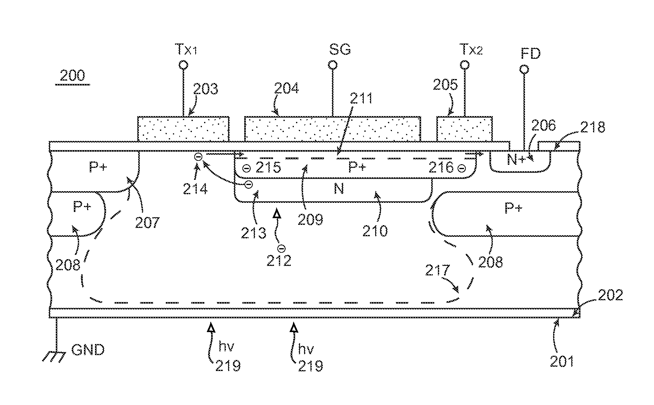
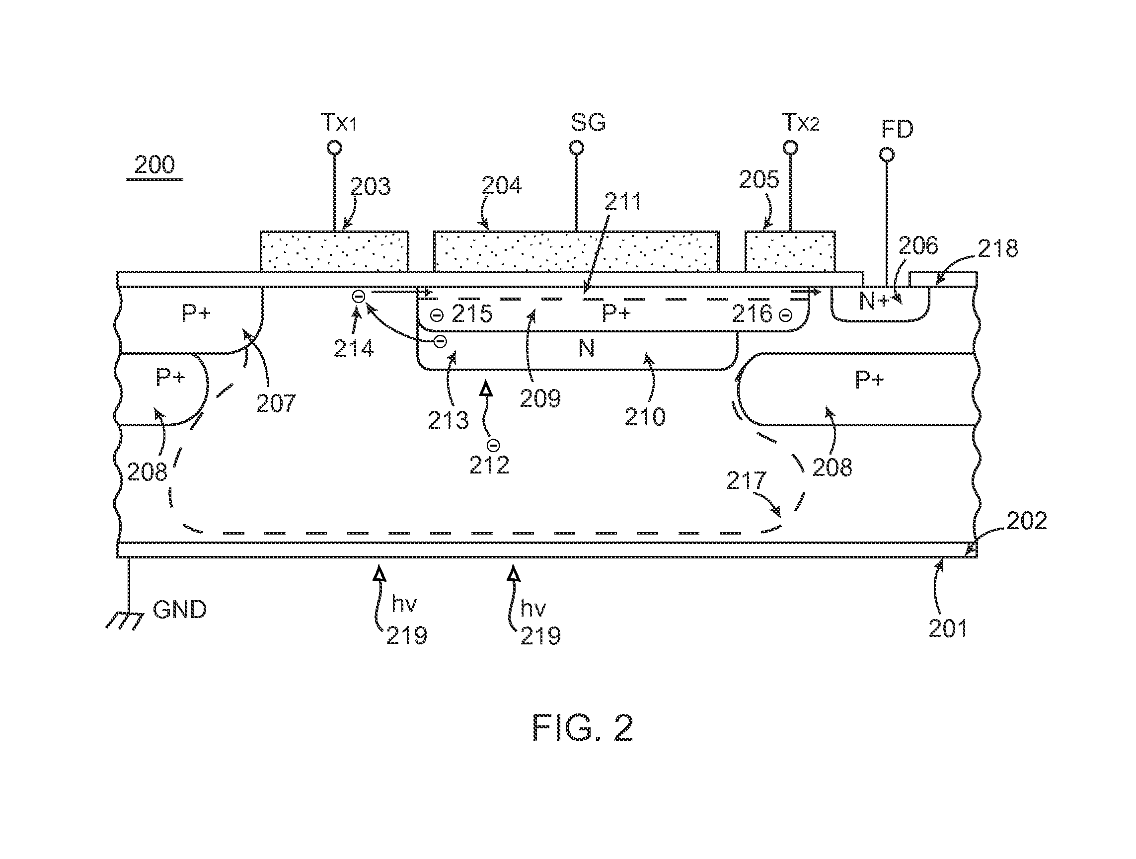
[0014]The present invention will be described with reference to FIG. 2 which represents the simplified device cross section of a CMOS sensor pixel 200. The pixel 200 consists of a pinned photodiode with a top storage gate 204. The pinned photodiode is formed by the p+ type doped layer 209 and the n type doped layer 210. The substrate 201 is p type doped and has a p+ type doped layer 202 deposited near the back surface. This layer 202 helps suppress dark current generation in that area. The top surface of the structure has an insulating layer 218, preferably silicon dioxide, grown on it that serves as the gate insulator for poly-silicon gates 203, 204 and 205. Gate 203 is the transfer gate Tx1, which is used to transfer accumulated electron charge 213 from the pinned photodiode to an area under the gate 203 as charge 214, when this gate 203 is pulsed positive. After the gate bias returns to its original bias level, which is zero or slightly negative, electron charge 214 is then trans...


PUM


Abstract

The invention describes a solid-state CMOS image sensor array and in particular describes in detail the image sensor array pixels, with global and rolling shutter capabilities, that utilize charge storage gates located on top of a pinned photodiode. The sensor array is illuminated from the back side and the location of the storage gate on top of the pinned photodiode saves valuable pixel area, which does not compromise the Dynamic Range of the image sensor.

Description

CROSS REFERENCE TO RELATED APPLICATION[0001]This application claims priority under 35 USC Sec. 119 (e)(1) of provisional application No. 61 / 438,785 filed on Feb. 2, 2011.BACKGROUND OF THE INVENTION[0002]1. Field of the Invention[0003]The present invention relates to back side illuminated solid-state image sensors, and more particularly to small pixel size, back side illuminated CMOS image sensors having both global shutter (GS) and rolling shutter (RS) capabilities.[0004]2. Discussion of Related Art[0005]Typical image sensors sense light by converting impinging photons into electrons that are integrated (collected) in sensor pixels. After completion of an integration cycle collected charge is converted into a voltage, which is supplied to the output terminals of the sensor. In CMOS image sensors the charge to voltage conversion is accomplished directly in the pixels themselves and the analog pixel voltage is transferred to the output terminals through various pixel addressing and sc...

Claims


Application Information

Patent Timeline
Patent Type & Authority Patents(United States)
IPC IPC(8): H01L21/00
CPCH01L27/146H01L21/00H01L31/103H01L31/12H01L27/14612H01L27/14806
Inventor HYNECEK, JAROSLAV
Owner APTINA IMAGING CORP
Why Eureka
Try Eureka