
Light emitting diode package structure

a technology of light-emitting diodes and package structures, which is applied in the direction of basic electric elements, electrical equipment, semiconductor devices, etc., can solve the problems of limited light extraction efficiency of light-emitting diodes

Active Publication Date: 2014-05-27
LEXTAR ELECTRONICS CORP
View PDF1 Cites 1 Cited by
  • Summary
  • Abstract
  • Description
  • Claims
  • Application Information

AI Technical Summary

Benefits of technology

The composite coating layer effectively reduces light trapping, improving light extraction efficiency by increasing reflectivity and transmission, while the wavelength transformation material enhances the output light spectrum.

Problems solved by technology

Therefore, the light extraction efficiency of the light emitting diode is limited.

Method used


Image

  • Light emitting diode package structure
  • Light emitting diode package structure
  • Light emitting diode package structure

Examples


second embodiment

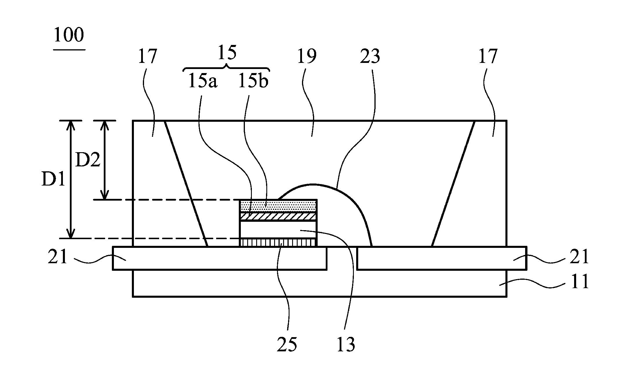
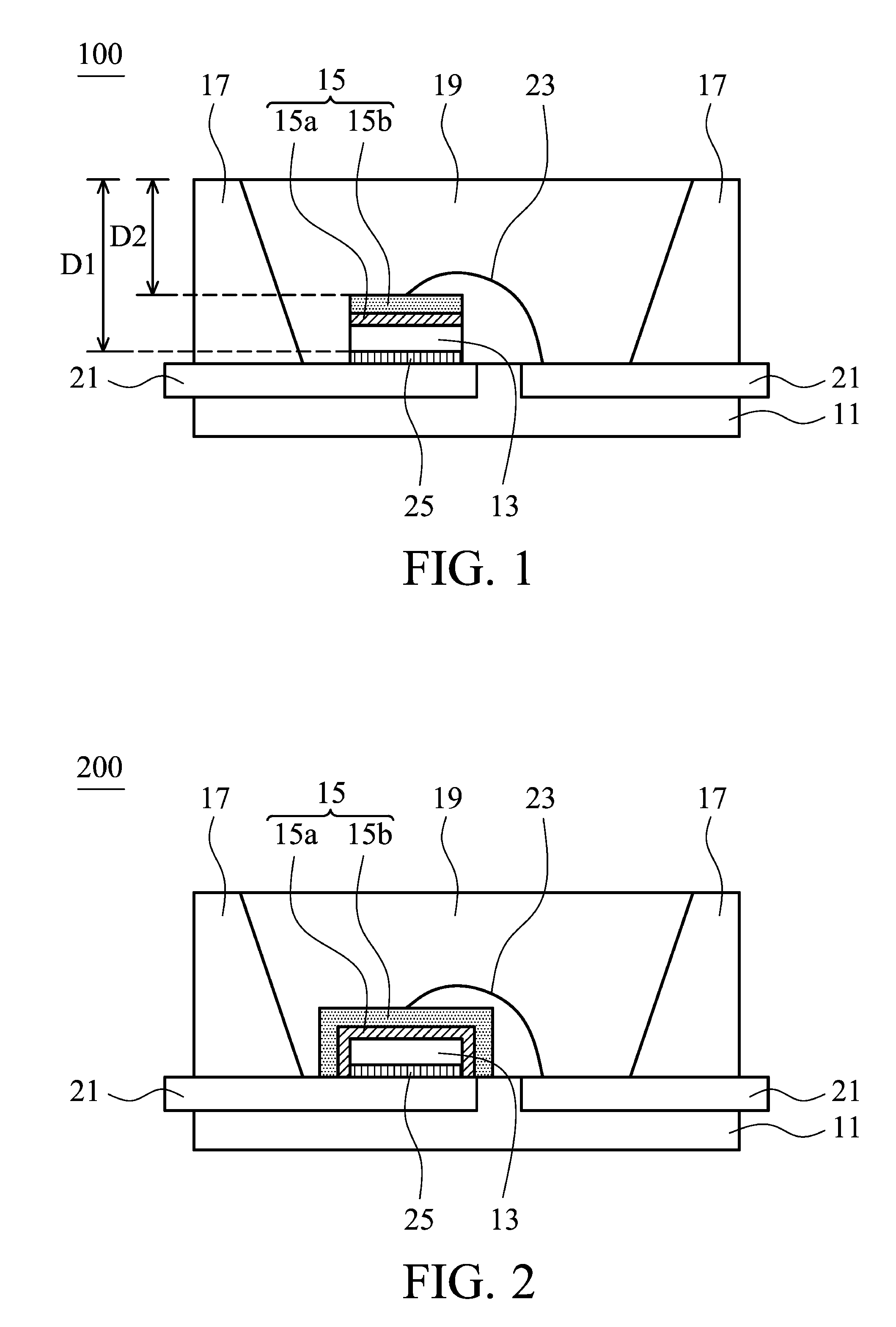
[0024]Furthermore, FIG. 2 shows a cross-sectional schematic representation of a light emitting diode package structure 200 in accordance with the invention. Besides being formed on the light emitting diode chip 13, a portion of the composite coating layer 15 is formed on the sidewalls of the light emitting diode chip. In other words, the composite coating layer 15 is formed on the five surfaces of the light emitting diode chip 13 (top surface and four sidewalls).

third embodiment

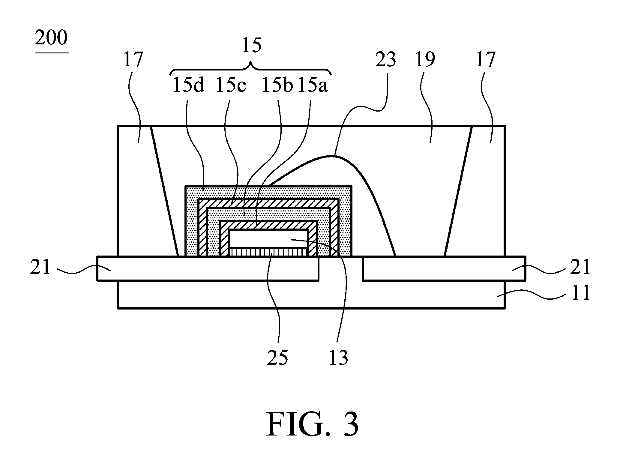
[0025]Furthermore, FIG. 3 shows a cross-sectional schematic representation of a light emitting diode package structure in accordance with the invention. The composite coating layer 15 further comprises a third coating layer 15c and a fourth coating layer 15d, the first coating layer 15a and the third coating layer 15c are formed of the same material, and the second coating layer 15b and the fourth coating layer 15d are formed of the same material. Note that the composite coating layer 15 may comprise two layers, four layers, six layers, eight layers or multi-layers, and is not limited by the above-mentioned numbers. Note that two adjacent coating layers must have different refractive indexes, and the number and the thickness of the composite coating layer may be adjusted by those skilled in the art according to the actual application.

[0026]The encapsulation housing 19 comprises a wavelength transformation material, such as a phosphor powder, quantum dot or organic emitting material....


PUM


Abstract

The invention provides a light emitting diode package structure, including: a light emitting diode chip formed on a substrate; a composite coating layer formed on the light emitting diode chip, wherein the composite coating layer comprises a first coating layer and a second coating layer, and the composite coating layer has a reflectivity greater than 95% at the wavelength of 500-800 nm; a cup body formed on the substrate, wherein the cup body surrounds the light emitting diode chip; and an encapsulation housing covering the light emitting diode chip, wherein the encapsulation housing comprises a wavelength transformation material.

Description

CROSS REFERENCE TO RELATED APPLICATIONS[0001]This Application claims priority of Taiwan Patent Application No. 100108668, filed on Mar. 15, 2011, the entirety of which is incorporated by reference herein.BACKGROUND OF THE INVENTION[0002]1. Field of the Invention[0003]The present invention relates to a light emitting diode, and in particular relates to a light emitting diode package structure.[0004]2. Description of the Related Art[0005]Because light emitting diodes (LED) have several advantages over conventional lamps, such as a longer lifetime, a smaller size, lower power consumption, and higher response speeds, etc., considerable research attention has been recently focused on development thereof.[0006]Conventionally, one way to generate a white light emitting diode (LED) is to coat a yellow phosphor on a blue LED chip. The blue light emitted by the LED chip is then mixed with the complimentary yellow light from phosphor to generate the white light. An LED comprises a semiconducto...

Claims


Application Information

Patent Timeline
Patent Type & Authority Patents(United States)
IPC IPC(8): H01L33/00
CPCH01L33/50H01L33/46H01L2224/48091H01L2224/48247H01L2224/8592H01L2924/00014
Inventor CAI, PEI-SONGLIN, TZU-PUFU, SZU-WEI
Owner LEXTAR ELECTRONICS CORP
Learn More