Wafer level package structure and fabrication methods

a technology of package structure and fabrication method, applied in the field of integrated circuit packaging, can solve the problems of adversely affecting the yield, wlp suffers drawbacks, and the packaging of semiconductor dies becomes more difficult, and achieves the effect of reducing the damage to semiconductor chips caused by the formation of stud bumps

Active Publication Date: 2014-06-24
TAIWAN SEMICON MFG CO LTD
View PDF8 Cites 479 Cited by
  • Summary
  • Abstract
  • Description
  • Claims
  • Application Information

AI Technical Summary

Benefits of technology

[0011]An advantageous feature of the present invention is that since stud bumps are formed on package substrates, the damage to semiconductor chips caused by the formation of stud bumps is reduced.

Problems solved by technology

As a result, the packaging of the semiconductor dies becomes more difficult, adversely affecting the yield.
However, WLP suffers drawbacks.
With the limited areas of the dies, the number of the I / O pads is limited due to the limitation of the pitch of the I / O pads.
Additionally, under the fixed ball-size requirement, solder balls must have a certain size, which in turn limits the number of solder balls that can be packed on the surface of a die.
These packaging techniques suffer from a common drawback: the dies have to be aligned to their respective connecting portions with very high accuracy.
Otherwise, the package may fail.

Method used


Image

  • Wafer level package structure and fabrication methods
  • Wafer level package structure and fabrication methods
  • Wafer level package structure and fabrication methods

Examples


Embodiment Construction

[0015]The making and using of the presently preferred embodiments are discussed in detail below. It should be appreciated, however, that the present invention provides many applicable inventive concepts that can be embodied in a wide variety of specific contexts. The specific embodiments discussed are merely illustrative of specific ways to make and use the invention, and do not limit the scope of the invention.

[0016]A novel package structure and methods of forming the same are provided. The intermediate stages of manufacturing a preferred embodiment of the present invention are illustrated. Throughout the various views and illustrative embodiments of the present invention, like reference numbers are used to designate like elements.

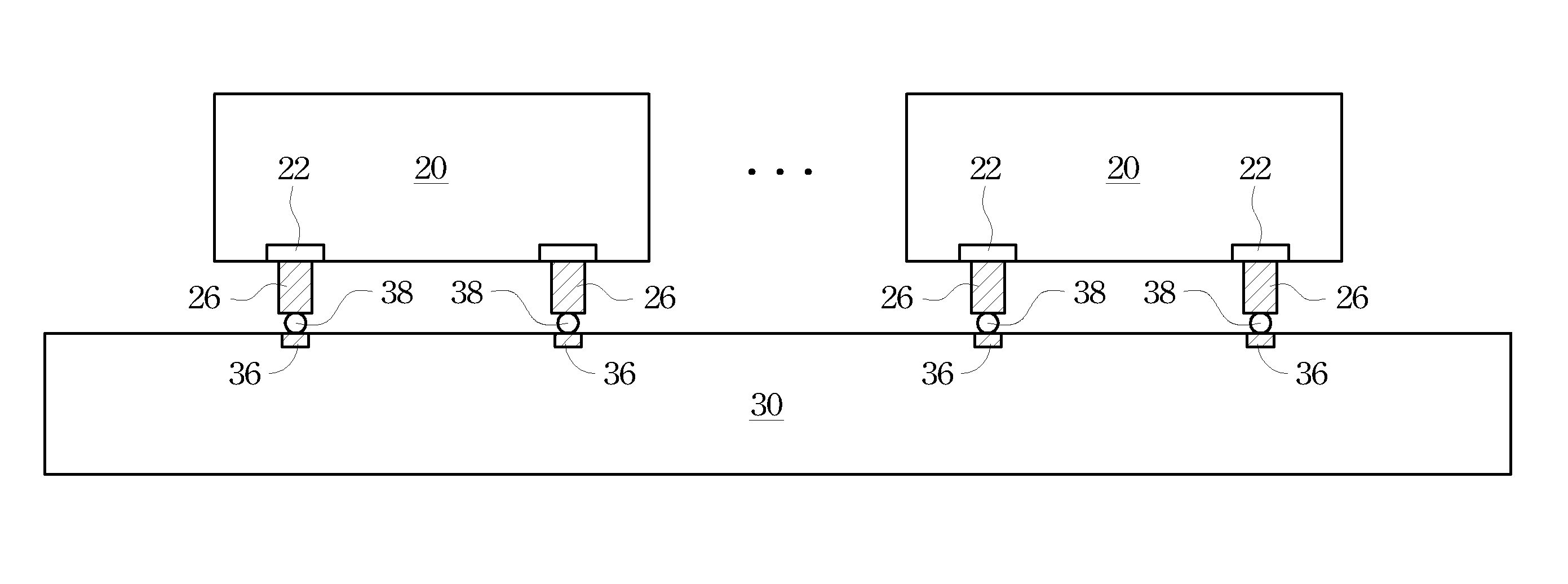
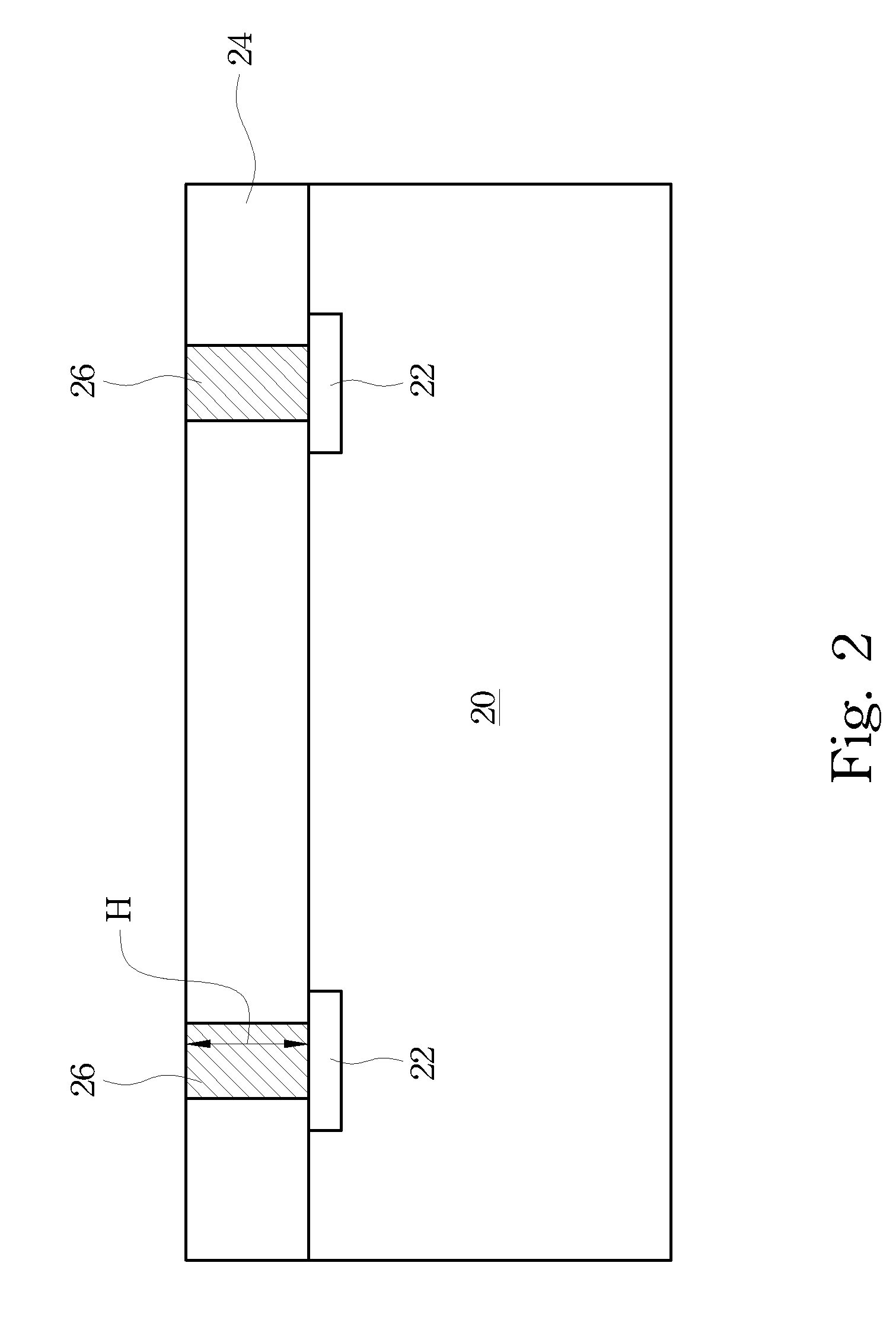
[0017]Referring to FIG. 2, die 20 is provided. Die 20 preferably includes a semiconductor substrate having integrated circuits and overlying interconnect structures (not shown) formed therein. Bond pads 22 are formed on the top surface of die 20, and are ...


PUM


Abstract

A method of forming a package structure with reduced damage to semiconductor dies is provided. The method includes providing a die comprising bond pads on a top surface of the die; forming bumps on the bond pads of the die, wherein the bumps have top surfaces higher than the top surface of the die; mounting the die on a chip carrier, wherein the bumps are attached to the chip carrier; molding the die onto the chip carrier with a molding compound; de-mounting the chip carrier from the die; and forming redistribution traces over, and electrically connected to, the bumps of the die.

Description

TECHNICAL FIELD[0001]This invention relates generally to integrated circuits, and more particularly to the packaging of integrated circuits.BACKGROUND[0002]With the evolving of semiconductor technologies, semiconductor dies are becoming increasingly smaller. However, more functions need to be integrated into the semiconductor dies. Accordingly, the semiconductor dies need to have increasingly greater numbers of I / O pads packed into smaller areas, and the density of the I / O pads rises quickly. As a result, the packaging of the semiconductor dies becomes more difficult, adversely affecting the yield.[0003]Package technologies can be divided into two categories. One category is typically referred to as wafer level package (WLP), wherein dies on a wafer are packaged before they are sawed. The WLP technology has some advantages, such as greater throughput and lower cost. Further, less under-fill or molding compound is needed. However, WLP suffers drawbacks. As aforementioned, the sizes o...

Claims


Application Information

Patent Timeline
Patent Type & Authority Patents(United States)
IPC IPC(8): H01L21/00
CPCH01L2924/01047H01L24/13H01L2924/01013H01L24/97H01L2924/00013H01L2924/14H01L2924/01078H01L21/568H01L2224/13099H01L2924/15311H01L2224/16H01L2224/0401H01L24/96H01L23/3107H01L2224/12105H01L21/561H01L24/19H01L24/10H01L21/6835H01L2224/04105H01L2224/20H01L2924/01029H01L2224/97H01L2924/01033H01L2224/13H01L2924/181H01L2224/82H01L2224/29099H01L2924/00
Inventor PU, HAN-PINGLII, MIRNG-JI
Owner TAIWAN SEMICON MFG CO LTD
Why Eureka
Try Eureka