

Memory device and electronic device
a technology of electronic devices and memory devices, applied in the field of memory devices, can solve the problem of taking a long time for data writing, and achieve the effect of reducing the circuit area
- Summary
- Abstract
- Description
- Claims
- Application Information
AI Technical Summary
Benefits of technology
Problems solved by technology
Method used
Image

Examples
embodiment 1
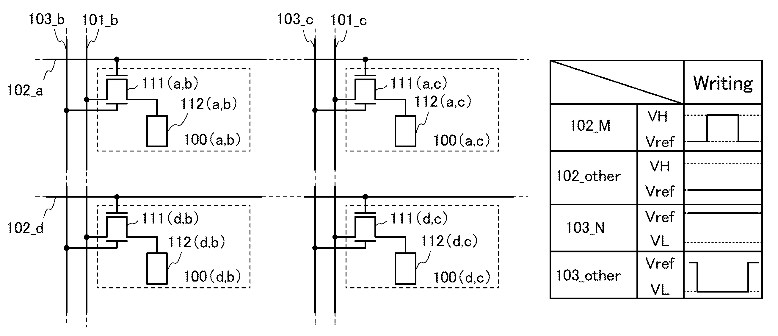
[0038]In this embodiment, an example of a memory device in which a selection operation can be performed for individual memory cells is described.
[0039]An example of the memory device in this embodiment includes three or more memory cells which are arranged in the row and column directions. The memory cells are provided in a memory cell array, for example.
[0040]An example of the memory device in this embodiment is described with reference to FIGS. 1A and 1B.
[0041]First, an example of a structure of the memory device in this embodiment is described with reference to FIG. 1A.
[0042]The memory device illustrated in FIG. 1A includes a memory cell 100 (a,b) (a and b are natural numbers), a memory cell 100 (a,c) (c is a natural number larger than a), a memory cell 100 (d,b) (d is a natural number larger than b), and a memory cell 100 (d,c). Note that the memory cell 100 (d,c) is not necessarily provided. Further, a memory cell other than the memory cell 100 (a,b), the memory cell 100 (a,c),...
embodiment 2
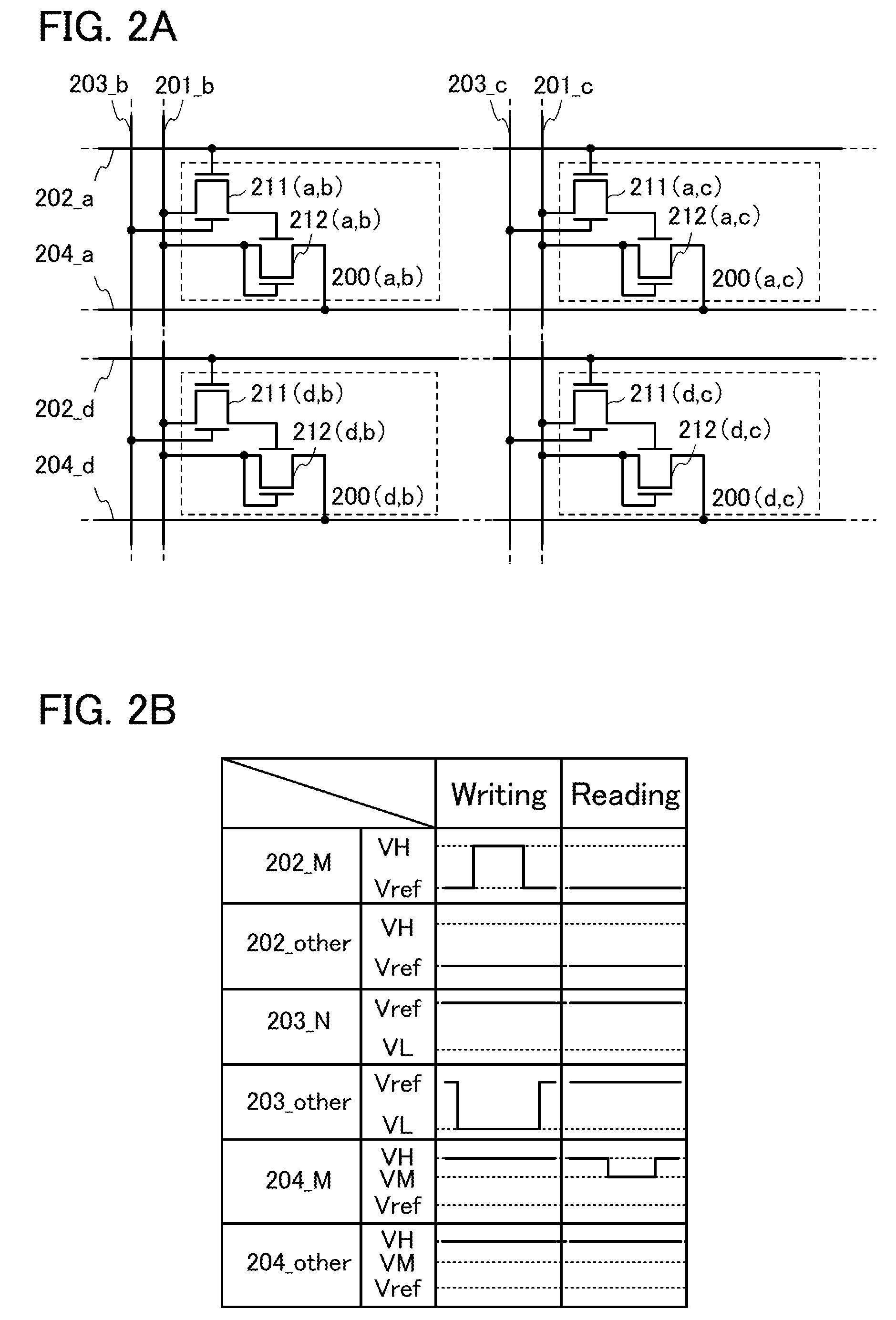
[0076]In this embodiment, an example of the memory device in Embodiment 1 is described.
[0077]An example of the memory device in this embodiment is described with reference to FIGS. 2A and 2B.
[0078]First, an example of a structure of the memory device in this embodiment is described with reference to FIG. 2A.
[0079]The memory device illustrated in FIG. 2A includes a memory cell 200 (a,b), a memory cell 200 (a,c), a memory cell 200 (d,b), and a memory cell 200 (d,c). Note that the memory cell 200 (d,c) is not necessarily provided. Further, a memory cell other than the memory cell 200 (a,b), the memory cell 200 (a,c), the memory cell 200 (d,b), and the memory cell 200 (d,c) may be provided. Further, a memory cell may be provided at any one or more of the following positions: between the memory cell 200 (a,b) and the memory cell 200 (a,c), between the memory cell 200 (a,b) and the memory cell 200 (d,b), between the memory cell 200 (d,b) and the memory cell 200 (d,c), and between the memo...
embodiment 3
[0127]In this embodiment, an example of a structure of a memory cell in the memory device in Embodiment 2 is described with reference to FIGS. 4A and 4B. FIGS. 4A and 4B illustrate an example of a structure of the memory cell in this embodiment. An example of a structure of the memory cell illustrated in FIGS. 2A and 2B is described here as an example. Note that the components illustrated in FIGS. 4A and 4B include those having sizes different from the actual sizes.
[0128]The memory cell illustrated in FIGS. 4A and 4B includes a conductive layer 751, an insulating layer 752, a semiconductor layer 753, a conductive layer 754a, a conductive layer 754b, an insulating layer 755, a conductive layer 756, a conductive layer 757, a conductive layer 758, an insulating layer 760, a semiconductor layer 761, a conductive layer 762a, a conductive layer 762b, an insulating layer 763, a conductive layer 764, a conductive layer 765, an insulating layer 766, and a conductive layer 767.
[0129]The condu...
PUM
 Abstract
Description
Claims
Application Information