Electronic device covered by multiple layers and method for manufacturing electronic device

a technology of electronic devices and layers, applied in the direction of microstructural devices, microstructural technology, microstructural systems, etc., can solve the problems of reducing reliability, affecting the reliability of electronic devices, so as to achieve high reliability and high reliability of electronic devices

Inactive Publication Date: 2014-08-05
SEIKO EPSON CORP
View PDF17 Cites 2 Cited by
  • Summary
  • Abstract
  • Description
  • Claims
  • Application Information

AI Technical Summary

Benefits of technology

[0007]An advantage of some aspects of the invention is to provide a highly reliable electronic device. Moreover, another advantage of some aspects of the invention is to provide a method for manufacturing the highly reliable electronic device.
[0009]According to the electronic device, compared with the case where, for example, a flat first covering layer covers the top of the cavity, it is possible to prevent the contact between the first covering layer and the MEMS structure due to an external impact or the like. Accordingly, the electronic device can have high reliability.
[0012]According to this configuration, when the inter-layer insulating layer is etched through the through-hole to release the MEMS structure, it is possible to prevent a step portion from being formed on the inner wall of the through-hole due to the difference in etching rate between the layers, compared with the case where, for example, the through-hole is formed in the second region where the number of stacked layers is large.
[0014]According to this configuration, the first covering layer can ensure conductivity while having high resistance to an etchant in releasing the MEMS structure.
[0022]According to the method for manufacturing the electronic device, it is possible to make the distance between the substrate and the first covering layer in the first region longer than the distance between the substrate and the first covering layer in the second region. Therefore, it is possible to prevent the contact between the first covering layer and the MEMS structure, whereby an electronic device with high reliability can be provided.
[0024]According to this configuration, when the inter-layer insulating layer is etched through the through-hole to release the MEMS structure, it is possible to prevent a step portion from being formed on the inner wall of the through-hole due to the difference in etching rate between the layers, compared with the case where, for example, the through-hole is formed in the second region where the number of stacked layers is large.

Problems solved by technology

However, such a problem that the MEMS structure and the first covering layer contact each other sometimes occurs due to an external impact or the like.
When the problem occurs, the MEMS structure cannot operate stably, thereby leading to a reduction in reliability.
Especially in recent years, the distance between the MEMS structure and the first covering layer becomes short in response to the demand for miniaturization of the electronic devices, which is likely to cause the problem described above.
For example, when the planar shape of the first region is quadrilateral, stress is concentrated on corners, and, therefore, it is sometimes difficult to stably displace the first covering layer in the first region upward.

Method used


Image

  • Electronic device covered by multiple layers and method for manufacturing electronic device
  • Electronic device covered by multiple layers and method for manufacturing electronic device
  • Electronic device covered by multiple layers and method for manufacturing electronic device

Examples


Embodiment Construction

[0037]Hereinafter, a preferred embodiment of the invention will be described with reference to the drawings.

1. Electronic Device

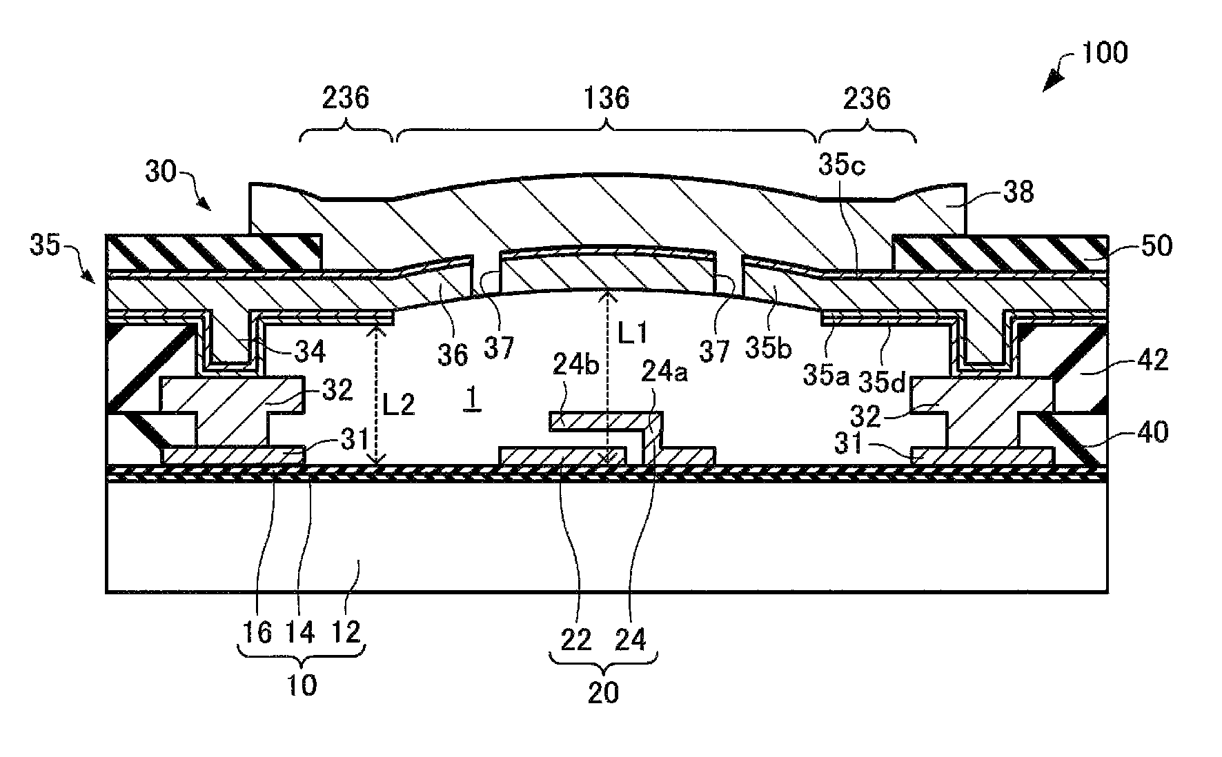
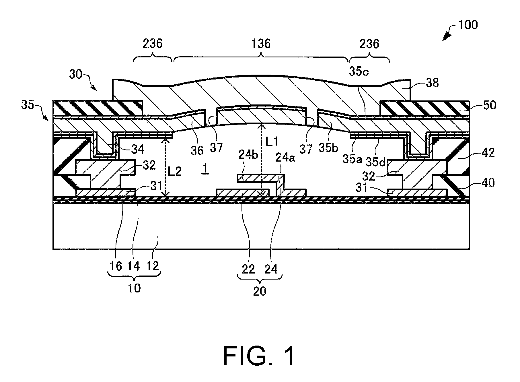
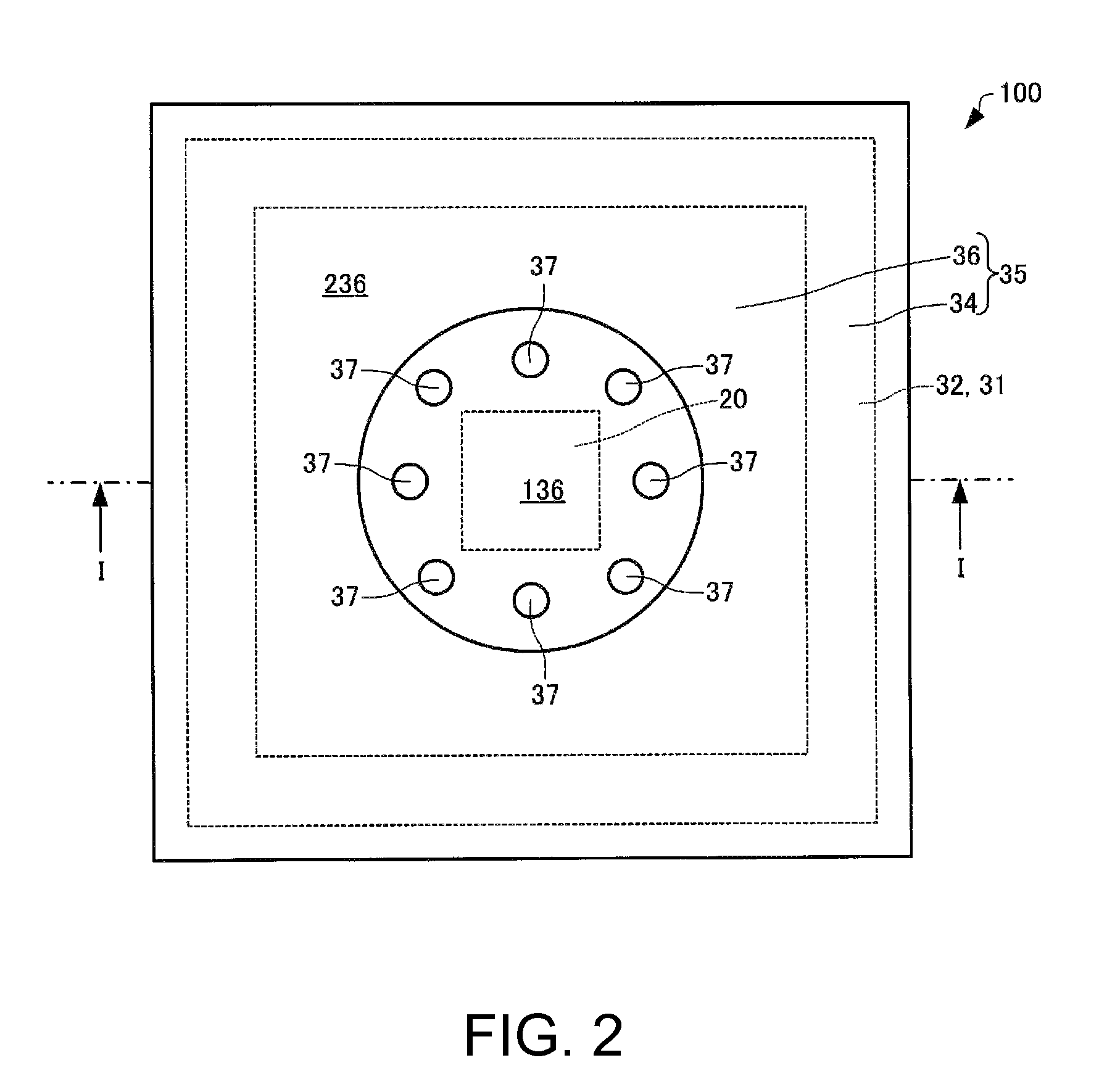
[0038]First, an electronic device according to an embodiment will be described with reference to the drawings. FIG. 1 is a cross-sectional view schematically showing the electronic device 100 according to the embodiment. FIG. 2 is a plan view schematically showing the electronic device 100 according to the embodiment. FIG. 3 schematically shows the electronic device 100 according to the embodiment. Here, FIG. 1 is a cross-sectional view taken along line I-I of FIG. 2. In FIG. 2, a second covering layer 38 and a passivation layer 50 are not illustrated for the sake of convenience. In FIG. 3, only an MEMS structure 20 and an oscillator circuit 60 are illustrated for the sake of convenience.

[0039]As shown in FIGS. 1 to 3, the electronic device 100 includes a substrate 10, the MEMS structure 20, and a covering structure 30. Further, the electronic device 100 ca...


PUM


Abstract

An electronic device according to the invention includes: a substrate; an MEMS structure formed above the substrate; and a covering structure defining a cavity in which the MEMS structure is arranged, wherein the covering structure has a first covering layer covering from above the cavity and having a through-hole in communication with the cavity and a second covering layer formed above the first covering layer and closing the through-hole, the first covering layer has a first region located above at least the MEMS structure and a second region located around the first region, the first covering layer is thinner in the first region than in the second region, and a distance between the substrate and the first covering layer in the first region is longer than a distance between the substrate and the first covering layer in the second region.

Description

BACKGROUND[0001]1. Technical Field[0002]The present invention relates to an electronic device and a method for manufacturing the electronic device.[0003]2. Related Art[0004]Electronic devices including a functional element, such as an MEMS (micro electro mechanical system), arranged in a cavity disposed on a substrate have been generally known. An MEMS, such as a microvibrator, a microsensor, or a microactuator, is housed in the cavity in an operable state because the minute structure needs to be arranged in such a state that it can vibrate, deform, or perform other motions.[0005]As a method for forming a cavity, JP-A-2009-188785 discloses a forming method in which an MEMS structure is formed on a substrate, an inter-layer insulating layer is formed on the MEMS structure, a first covering layer having through-holes is formed, the inter-layer insulating layer is removed through the through-holes of the first covering layer to release the MEMS structure, and, finally, the through-hole...

Claims


Application Information

Patent Timeline
Patent Type & Authority Patents(United States)
IPC IPC(8): H01L23/02H01L23/04H01L23/06
CPCB81B3/00B81B7/02B81C1/00H03B5/30H03H9/24B81C1/00333B81C2203/0145
Inventor KANEMOTO, YOKOSATO, AKIRAINABA, SHOGO
Owner SEIKO EPSON CORP
Why Eureka
Try Eureka