

Method for manufacturing electronic device, electronic device, and electronic apparatus
- Summary
- Abstract
- Description
- Claims
- Application Information
AI Technical Summary
Benefits of technology
Problems solved by technology
Method used
Image

Examples
first embodiment
of an Electronic Device
[0064]First, an active matrix device (thin-film transistor circuit) including an electronic device according to a first embodiment of the invention will be explained.
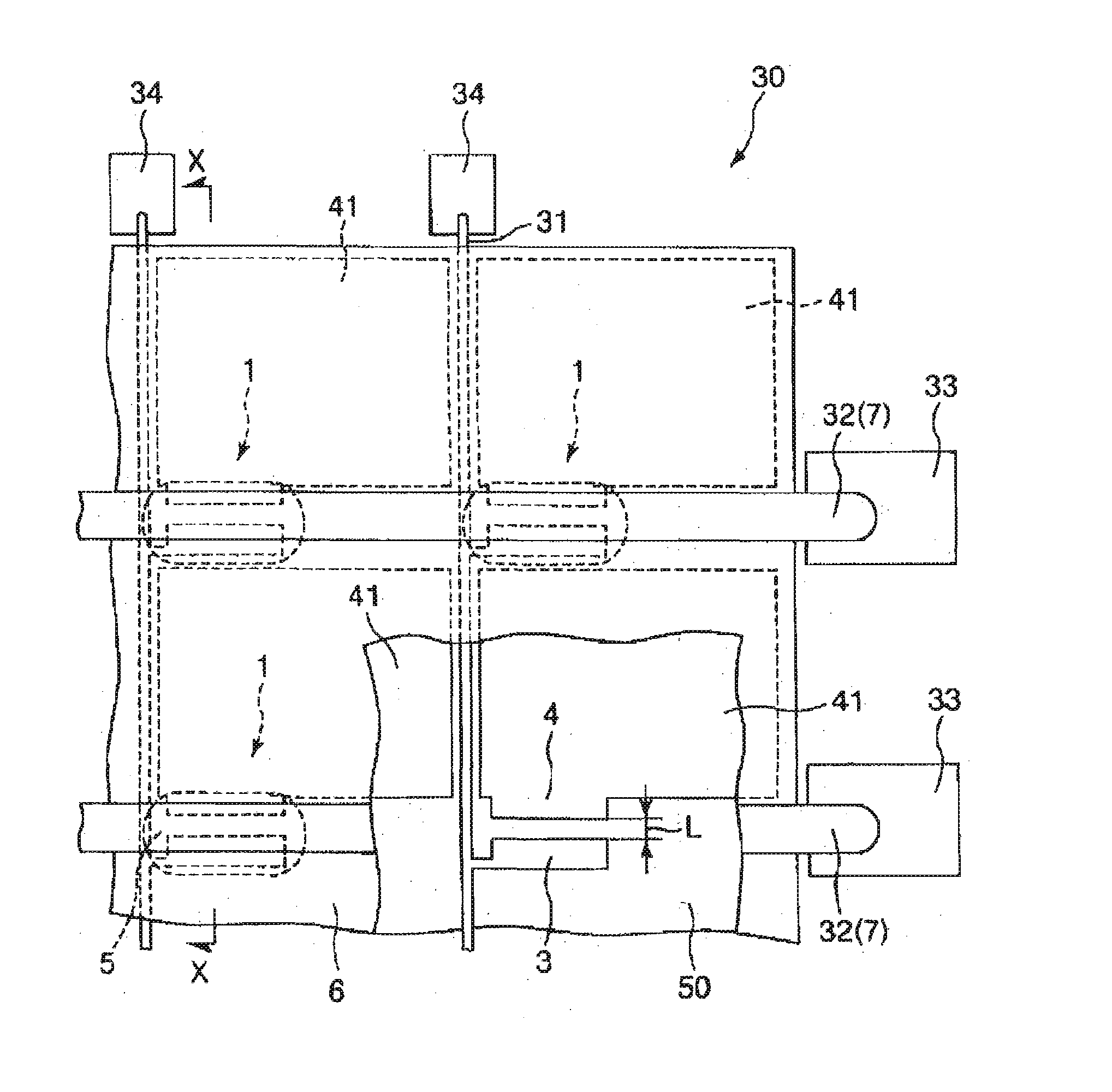
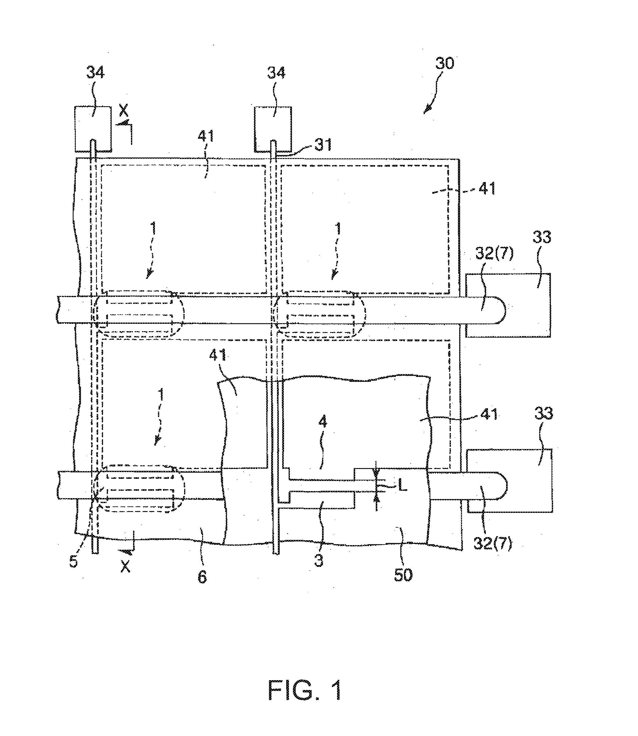
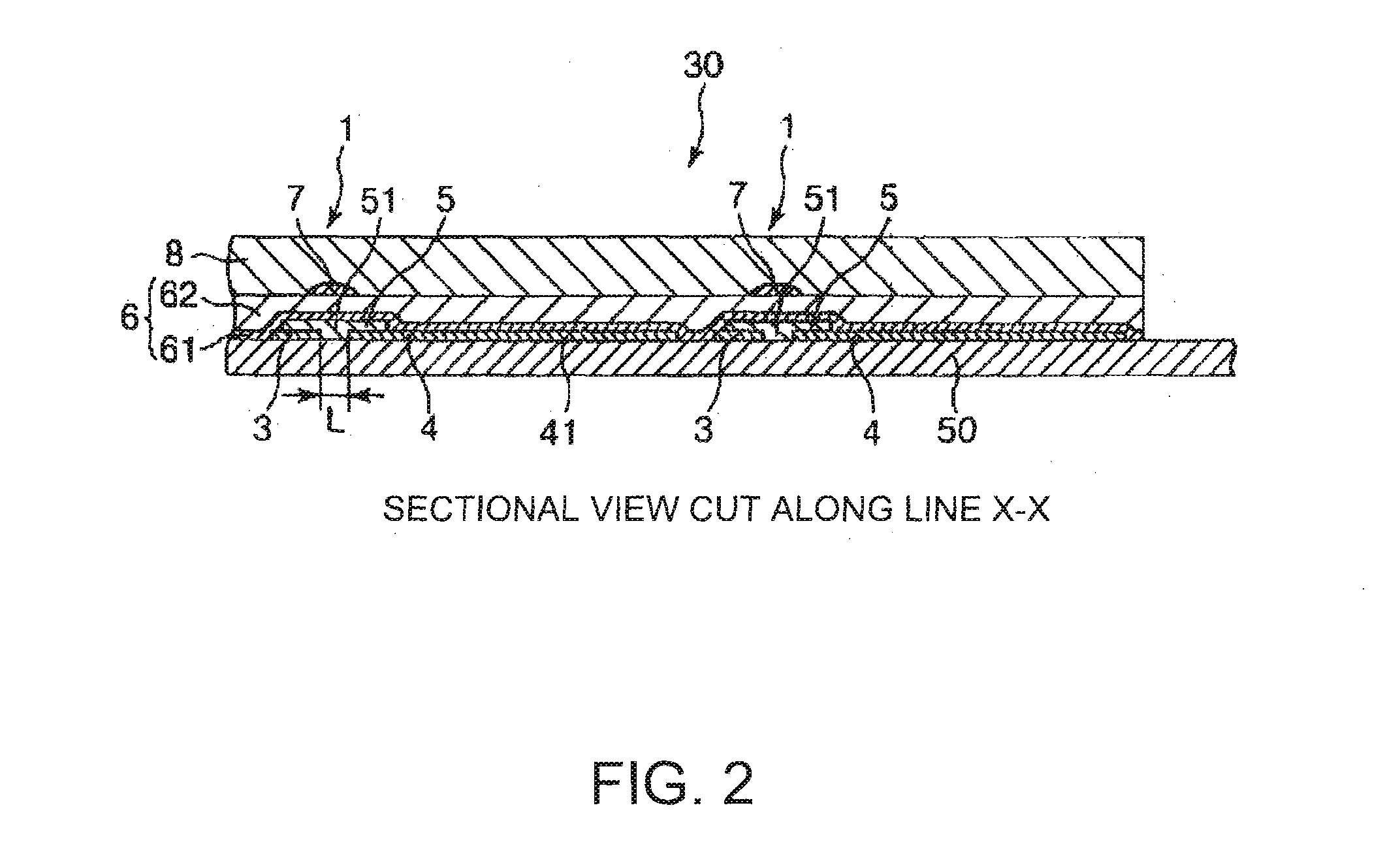
[0065]FIG. 1 is a plan view showing the active matrix device including the electronic device according to the first embodiment of the invention, while FIG. 2 is a sectional view cut along the line X-X shown in FIG. 1. In the following description, the top side in FIG. 2 is described as “up”, while the bottom side is described as “down”.
[0066]An active matrix device 30 shown in FIG. 1 includes a plurality of data lines 31, a plurality of scanning lines 32 perpendicular to the plurality of data lines, and a thin film transistor 1 provided adjacent to each of intersections of the data lines 31 and the scanning lines 32.
[0067]Each transistor 1 is provided with a source electrode 3, a drain electrode 4, an organic semiconductor layer 5, a gate insulating layer 6, and a gate electrode 7.
[0068]In this em...
second embodiment
of an Electronic Device
[0205]Next, a biosensor including an electronic device according to a second embodiment of the invention will be explained.
[0206]FIG. 6 is a schematic view (perspective view) showing a state in which the biosensor including the electronic device according to the second embodiment of the invention is attached to measuring equipment. FIG. 7 is a plan view schematically showing the biosensor shown in FIG. 6, while FIG. 8 is a sectional view of the biosensor shown in FIG. 7 cut along the line A-A. FIG. 9 is a partially enlarged view cut along the line A-A shown in FIG. 8. In the following description, the front side in FIG. 7 is described as “up”, while the back side is described as “down”. Further, the upper side of the FIGS. 8 and 9 is described as “top” and the lower side of the drawing is described as “bottom”.
[0207]The electronic device of the second embodiment (biosensor) and the method manufacturing it are described below. Each description is focused mainly...
PUM
 Abstract
Description
Claims
Application Information