Protection circuit, semiconductor device, photoelectric conversion device, and electronic device

a protection circuit and photoelectric conversion technology, applied in the direction of semiconductor devices, diodes, electrical devices, etc., to achieve the effect of high performance of suppressing the increase in esd potential, high reliability of photoelectric conversion, and high reliability of semiconductor devices

Inactive Publication Date: 2010-08-12
SEMICON ENERGY LAB CO LTD
View PDF106 Cites 12 Cited by
  • Summary
  • Abstract
  • Description
  • Claims
  • Application Information

AI Technical Summary

Benefits of technology

[0017]With the structure of the protection circuit which is one mode of the present invention, a protection circuit which has high performance of suppressing increase in the ESD potential can be obtained. In addition, a highly reliable semiconductor device, a highly reliable photoelectric conversion device, and a highly reliable electronic device can be obtained.

Problems solved by technology

However, in the case where the above signal line protection circuit of Patent Document 1 is employed and diodes in the protection circuit are provided between a signal line terminal (a SIG terminal) and a high potential power supply terminal (a VDD terminal) and between the SIG. terminal and a low potential power supply terminal (a VSS terminal), the following problem may be caused: when an operation in which a signal potential that is input to SIG. is higher than or equal to a VDD potential or lower than or equal to a VSS potential is performed, either of the diodes is forward-biased; accordingly, current flows and the signal potential becomes equal to the VSS potential or the VDD potential.

Method used


Image

  • Protection circuit, semiconductor device, photoelectric conversion device, and electronic device
  • Protection circuit, semiconductor device, photoelectric conversion device, and electronic device
  • Protection circuit, semiconductor device, photoelectric conversion device, and electronic device

Examples


embodiment 1

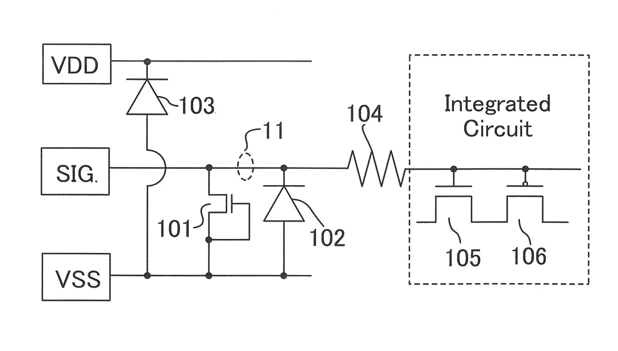
[0036]An embodiment of the present invention will be described below. Here, a protection circuit according to one mode of the present invention is applied to an integrated circuit using a semiconductor.

[0037]FIG. 1 illustrates a circuit including a signal line (SIG), a high potential power supply line (VDD), a low potential power supply line (VSS), and an integrated circuit (here, complementary transistors are illustrated as an example; however, one mode of the present invention is not limited thereto, and the same can be said for FIG. 2 and FIG. 3). In the case where a high potential signal of SIG. has a potential higher than that of VDD, a diode 102 and a diode-connected transistor 101 are provided between SIG. and VSS, a diode 103 is provided between VSS and VDD, and a resistor 104 connected in series is provided. This resistor connected in series is not necessarily provided.

[0038]By provision of the diode 102 and the diode 103, when a signal having a potential higher than that o...

embodiment 2

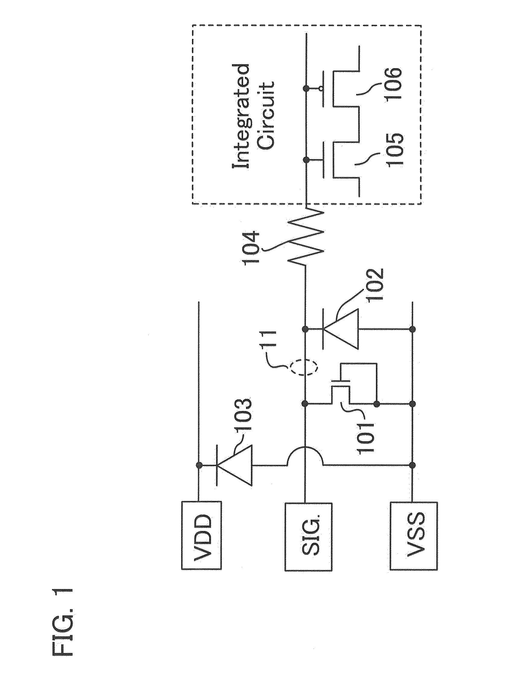
[0043]Another embodiment of the present invention will be described in a manner similar to that of Embodiment 1. Here, a protection circuit according to one mode of the present invention is applied to an integrated circuit using a semiconductor.

[0044]FIG. 2 illustrates an example of a configuration of a protection circuit provided for a signal line (SIG) for inputting a signal to an integrated circuit. The protection circuit includes a resistor 1203 provided in series between the signal line and the integrated circuit, a diode 1201 provided between SIG. and VSS, and a diode 1202 provided between VDD and VSS. Note that the resistor 1203 is not necessarily provided.

[0045]In the circuit of FIG. 2, when SIG. is negatively charged due to ESD, electric charges are released through the diode 1201 to the VSS side. When SIG is positively charged due to ESD, electric charges are released toward VDD, passing through the diode 1201, VSS, and the diode 1202.

[0046]Specifically, the circuit in FIG...

embodiment 3

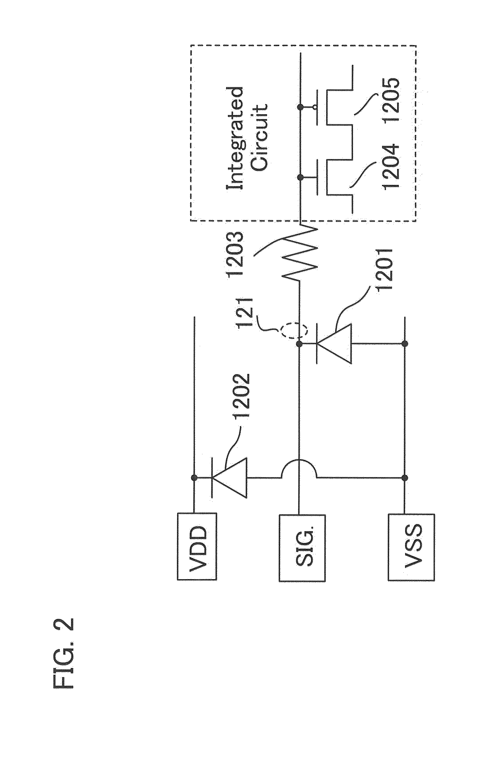
[0047]Another embodiment of the present invention will be described in a manner similar to those of Embodiment 1 and Embodiment 2. Here, a protection circuit according to one mode of the present invention is applied to an integrated circuit using a semiconductor.

[0048]FIG. 3 illustrates an example of a configuration of a protection circuit provided for a signal line (SIG) for inputting a signal to an integrated circuit. The protection circuit includes a resistor 1303 provided in series between the signal line and the integrated circuit, a diode-connected transistor 1301 provided between SIG. and VSS, and a diode 1302 provided between VDD and VSS. Note that the resistor 1303 is not necessarily provided.

[0049]In the circuit of FIG. 3, when SIG. is negatively charged due to ESD, electric charges are released through the diode-connected transistor 1301 to the VSS side. When SIG. is positively charged due to ESD, electric charges are released toward VDD, passing through the diode-connect...


PUM


Abstract

It is an object to provide a protection circuit and a semiconductor device to which a countermeasure against ESD is applied. The protection circuit includes a signal line electrically connected to an integrated circuit; a first diode provided between the signal line and a first power supply line; a second diode provided in parallel to the first diode; and a third diode provided between the first power supply line and a second power supply line. The first diode is a diode formed by diode-connecting a transistor, and the second diode is a diode having a PIN junction or a PN junction. The protection circuit is particularly effective when applied to a semiconductor device manufactured using a thin film transistor.

Description

BACKGROUND OF THE INVENTION[0001]1. Field of the Invention[0002]The present invention relates to a protection circuit.[0003]2. Description of the Related Art[0004]One of major causes of defects in an integrated circuit is damage to a semiconductor element, an electrode, or the like due to electrostatic discharge (hereinafter referred to as ESD). Thus, in order to prevent an integrated circuit from being damaged due to ESD, a protection circuit is provided between a terminal and the integrated circuit. A protection circuit refers to a circuit for preventing overvoltage applied to a terminal due to ESD or the like from being supplied to an integrated circuit.[0005]As for a protection circuit of a signal line, a technique for preventing overcurrent from flowing into an integrated circuit when a signal line terminal has a potential between that of a high potential power supply terminal (VDD) and that of a low potential power supply terminal (VSS) is disclosed in Patent Document 1.REFERE...

Claims


Application Information

Patent Timeline
Patent Type & Authority Applications(United States)
IPC IPC(8): H02H9/00
CPCH01L27/1225H01L27/0255H01L29/7869
Inventor SHISHIDO, HIDEAKIFUKUOKA, OSAMU
Owner SEMICON ENERGY LAB CO LTD
Why Eureka
Try Eureka