Method for manufacturing electronic device, electronic device, method for manufacturing electronic device package and electronic device package

a manufacturing method and electronic technology, applied in the direction of semiconductor devices, semiconductor/solid-state device details, electrical devices, etc., can solve the problems of difficult to obtain a highly reliable semiconductor package, difficult to accurately control the intensity or irradiation time of laser beams, etc., and achieve high-reliability electronic effects

Inactive Publication Date: 2012-09-13
SUMITOMO BAKELITE CO LTD
View PDF5 Cites 12 Cited by
  • Summary
  • Abstract
  • Description
  • Claims
  • Application Information

AI Technical Summary

Benefits of technology

[0013]According to the present invention, there are provided an electronic device manufacturing method capable of obtaining a highly

Problems solved by technology

However, in the case in which the molding material is irradiated with a laser beam, it is difficult to accurately control the intensity or irradiation time of

Method used


Image

  • Method for manufacturing electronic device, electronic device, method for manufacturing electronic device package and electronic device package
  • Method for manufacturing electronic device, electronic device, method for manufacturing electronic device package and electronic device package
  • Method for manufacturing electronic device, electronic device, method for manufacturing electronic device package and electronic device package

Examples


example 1

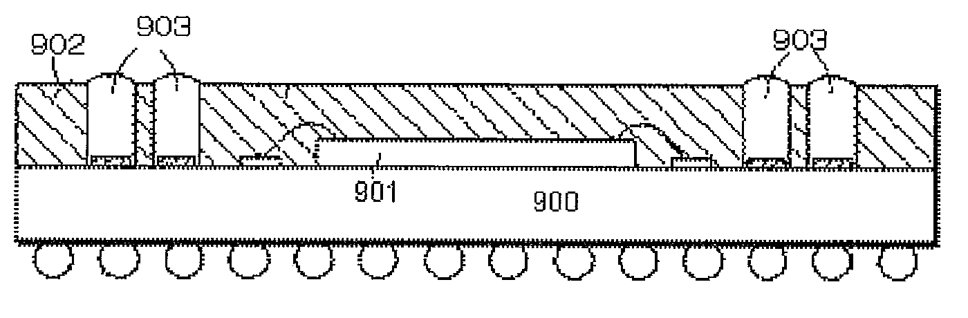
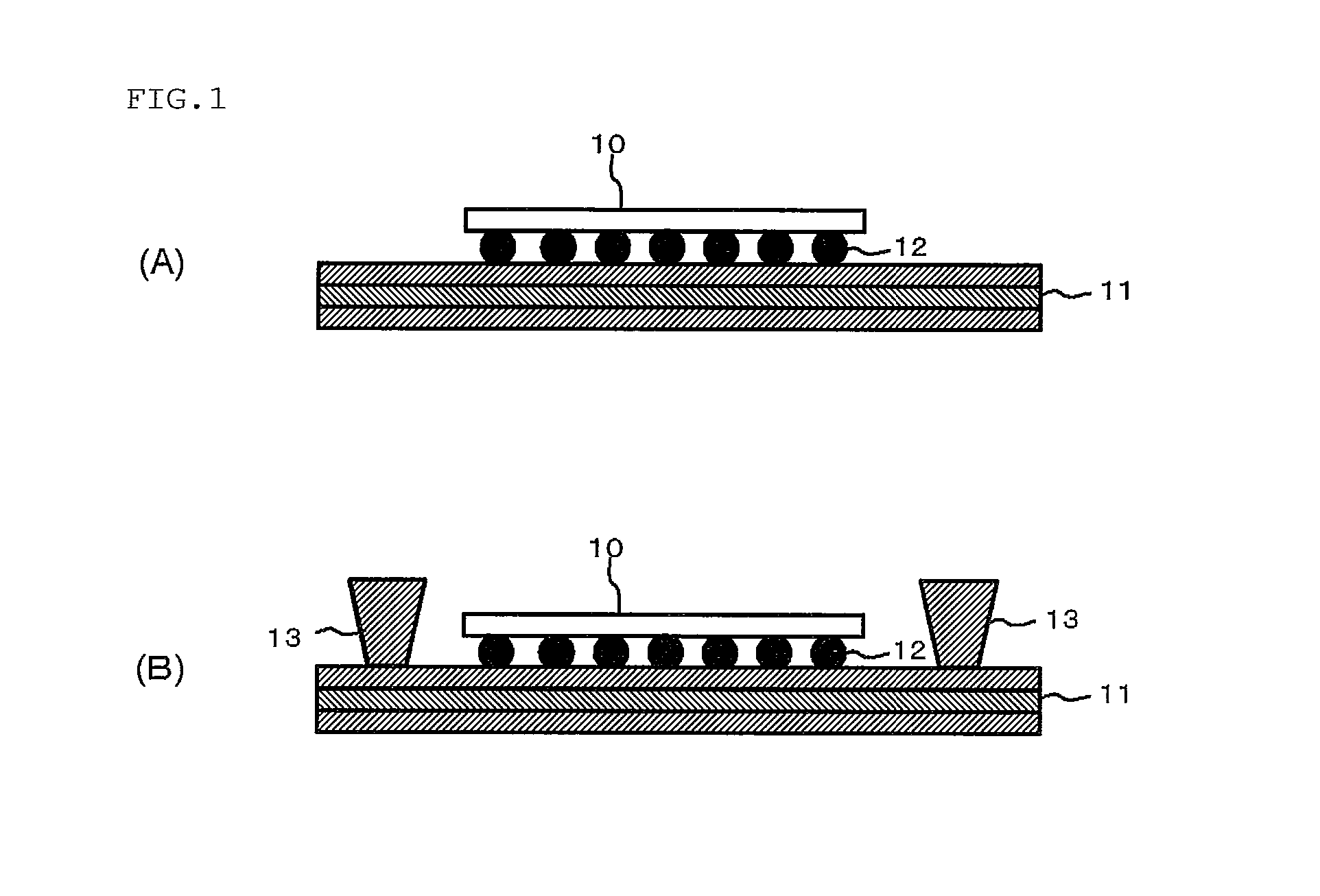
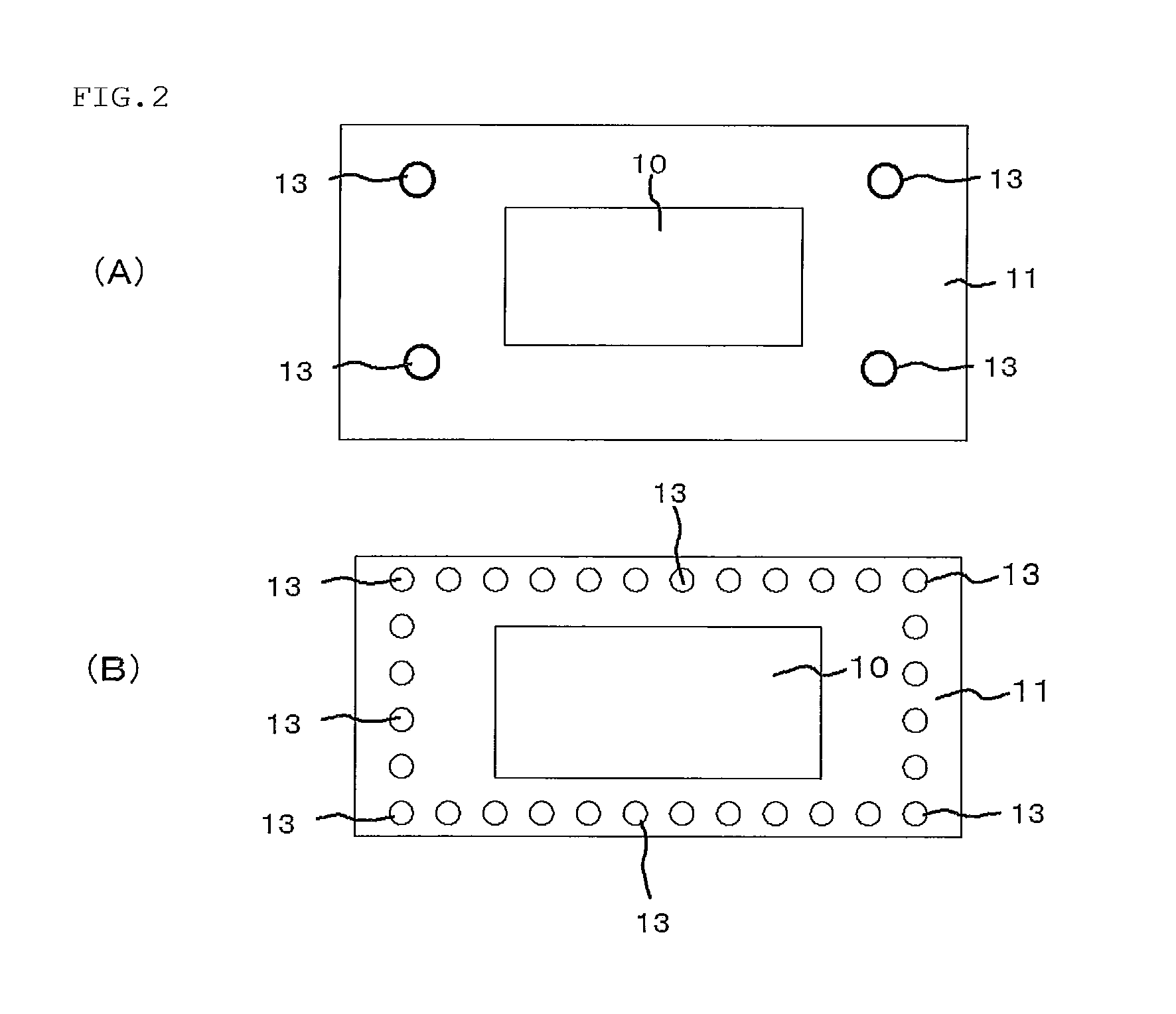
[0152]According to the same method as the above-described embodiment, standing portions were formed and holes were formed through an encapsulating material. Specifically, Example 1 was carried out in the following manner.

Synthesis of 1,4-polybuthylene Carbonate Resin

[0153]To a three-neck flask equipped with a stirrer, a raw material inlet and a nitrogen gas inlet, 1,4-butanediol (168 g, 1.864 mol) and diethyl carbonate (264.2 g, 2.236 mol) were added and the mixture was dissolved by heating to a temperature of 90 to 100° C. in a nitrogen atmosphere. Then, a 20% sodium ethoxide ethanol solution (80 ml, 0.186 mol) was added thereto, and the mixture was stirred at 90 to 100° C. in a nitrogen atmosphere for 1 hour. Then, the internal pressure of the reactor was reduced to about 30 kPa, followed by stirring at 90 to 100° C. for 1 hour and at 120° C. for 1 hour. Then, the reaction solution was stirred under a vacuum of 0.1 kPa at 150° C. for 1 hour and at 180° C. for 2 hours.

[0154]The re...

example 2

Preparation of Thermally Decomposable Resin Composition

[0165]The 1,4-polybuthylene carbonate obtained in Example 1 was dissolved in 150 g of anisole (solvent) to prepare a thermally decomposable resin composition having a resin concentration of 40%.

Formation of Standing Portions, Application of Encapsulating Material and Curing of Encapsulating Material

[0166]The formation of standing portions, the application of an encapsulating material and the curing of the encapsulating material were carried out in the same manner as described in Example 1.

Removal of Standing Portions (Formation of Holes)

[0167]Then, a sample for evaluation was thermally treated at 320° C. for 30 minutes while the thermally decomposable resin composition constituting the standing portions were thermally decomposed to leave holes.

[0168]The resulting sample was observed with a stereoscopic microscope, and as a result, the residue of the thermally decomposable resin composition was not observed on the surface of t...


PUM


Abstract

Disclosed is a method for manufacturing an electronic device, the method including: placing an electronic component on a substrate 11; forming standing portions 13 on the surface of the substrate 11 on which the electronic component 10 is placed, the standing portions 13 comprising a thermally decomposable resin; applying an encapsulating material 14 so as to encapsulate the electronic component 10 and cover around the standing portions 13 while exposing a portion of each of the standing portions 13 from the surface of the encapsulating material 14; heating the standing portions 13 to decompose and remove the standing portions 13, thereby forming holes 141 through the encapsulating material 14; and placing a conductive material 15 in the holes 141.

Description

TECHNICAL FIELD[0001]The present invention relates to a method for manufacturing an electronic device, an electronic device, a method for manufacturing an electronic device package and an electronic device package.BACKGROUND ART[0002]With the recent requirements of higher functionality, lightness, thinning, miniaturization and compactization in electronic devices, high-density integration and high-density mounting of electronic components are in progress.[0003]As a semiconductor device for high-density mounting, there has been proposed a semiconductor package having a package-on-package (POP) structure, in which a first semiconductor element is mounted on a substrate, and a substrate having a second semiconductor element mounted thereon is placed over the first semiconductor device.[0004]As the semiconductor device comprising the first semiconductor element which is used in the semiconductor package having the POP structure, a structure as shown in FIG. 8 has been proposed (see, for...

Claims


Application Information

Patent Timeline
IPC IPC(8): H01L21/56H01L23/28
CPCH01L21/565H01L23/3128H01L2924/3025H01L2225/1058H01L2225/1023H01L2224/73265H01L2924/3511H01L2224/32225H01L2924/01087H01L2924/01019H01L2924/15331H01L2924/15311H01L2924/01079H01L2924/01078H01L2924/01012H01L2924/01004H01L2224/73204H01L2224/48227H01L2224/48091H01L2224/16225H01L25/50H01L25/105H01L24/73H01L23/49811H01L23/49816H01L24/16H01L24/48H01L2924/00014H01L2924/00H01L2924/00012H01L2224/451H01L2924/12042H01L2924/181H01L2224/45099H01L2224/45015H01L2924/207H01L23/12H01L25/10H01L25/11
Inventor KAWATA, MASAKAZUTAKEUCHI, ETSUKUSUNOKI, JUNYASUGIYAMA, HIROMICHI
Owner SUMITOMO BAKELITE CO LTD
Why Eureka
Try Eureka