Adaptive voltage scalers (AVS), systems, and related methods

a voltage scaler and voltage level technology, applied in the field of adaptive voltage scalers, can solve the problems of delay variations, increase power consumption, and decrease in voltage level the maximum operating frequency of the circuit, so as to avoid or reduce tolerance voltage margins, and populated more quickly

Active Publication Date: 2014-08-05
QUALCOMM INC
View PDF24 Cites 7 Cited by
  • Summary
  • Abstract
  • Description
  • Claims
  • Application Information

AI Technical Summary

Benefits of technology

[0009]In one embodiment, the AVS comprises at least one delay circuit configured to receive an input signal. The AVS delays the input signal by a delay amount relating to at least one delay path of a functional circuit to produce a delay output signal. The AVS also comprises an AVS circuit coupled to an AVS database. The AVS circuit is responsive to the delay output signal. The AVS circuit is configured to generate a voltage level setting signal based on a voltage level in the database associated with an operating frequency for the functional circuit and delay information in the delay output signal. The AVS database can be configured to store voltage levels for various operating frequencies of a functional circuit(s) to avoid or reduce voltage margin.
[0011]The minimum voltage level settings in the AVS database may be configured to provide a voltage level with a tolerance voltage margin to avoid risking operating the functional circuit(s) in an invalid region of operation. However, in another embodiment, the AVS circuit is configured to explore the invalid region of operation of the functional circuit(s) during run-time operation to further avoid or reduce the tolerance voltage margin. In this embodiment, the AVS may comprise at least one delay circuit configured to receive an input signal and delay the input signal by an amount relating to at least one delay path of a functional circuit to produce a delay output signal. The AVS may also comprise an AVS circuit responsive to the delay output signal. The AVS circuit may be configured to generate a voltage level setting signal based on a target operating frequency for the functional circuit and delay information in the delay output signal. The AVS circuit may also be configured to increase the delay of the at least one delay path to simulate an increased operating frequency for the functional circuit to explore an invalid region of operation of the functional circuit. The point of transition to the invalid region of operation can be used by the AVS circuit to determine a revised voltage level setting for the current operating frequency to further avoid or reduce the tolerance voltage margin.
[0012]In another embodiment, the AVS circuit can be configured to accelerate population of the AVS database with voltage level settings for given operating frequencies. Once the AVS circuit learns a voltage level for a current operating frequency, the AVS circuit consults the voltage levels for lower operating frequencies in the AVS database. If the voltage levels stored for lower operating frequencies are greater than the learned voltage level for the current operating frequency, the AVS circuit can replace the voltage level for the lower operating frequencies with the learned lower voltage level in the AVS database. The functional circuit(s) is known to be able to properly operate at the learned voltage level for lower operating frequencies. In this manner, the AVS database is populated more quickly with lower voltage settings, if possible, so that voltage margin is more quickly avoided or reduced during operation.

Problems solved by technology

Thus, an increase in operating frequency generally results in more power consumption.
However, a decrease in voltage level decreases the maximum operating frequency possible for the circuit.
For example, variability in nanometer integrated circuit (IC) processes used to manufacture synchronous digital circuits and their components can cause delay variations.
Environmental conditions, such as operating temperature and aging effect of transistors, can affect propagation delay.
Voltage levels supplied by voltage supplies can be momentarily lowered due to variations in current draw, thus momentarily lowering performance.

Method used


Image

  • Adaptive voltage scalers (AVS), systems, and related methods
  • Adaptive voltage scalers (AVS), systems, and related methods
  • Adaptive voltage scalers (AVS), systems, and related methods

Examples


Embodiment Construction

[0040]With reference now to the drawing figures, several exemplary embodiments of the present disclosure are described. The word “exemplary” is used herein to mean “serving as an example, instance, or illustration.” Any embodiment described herein as “exemplary” is not necessarily to be construed as preferred or advantageous over other embodiments.

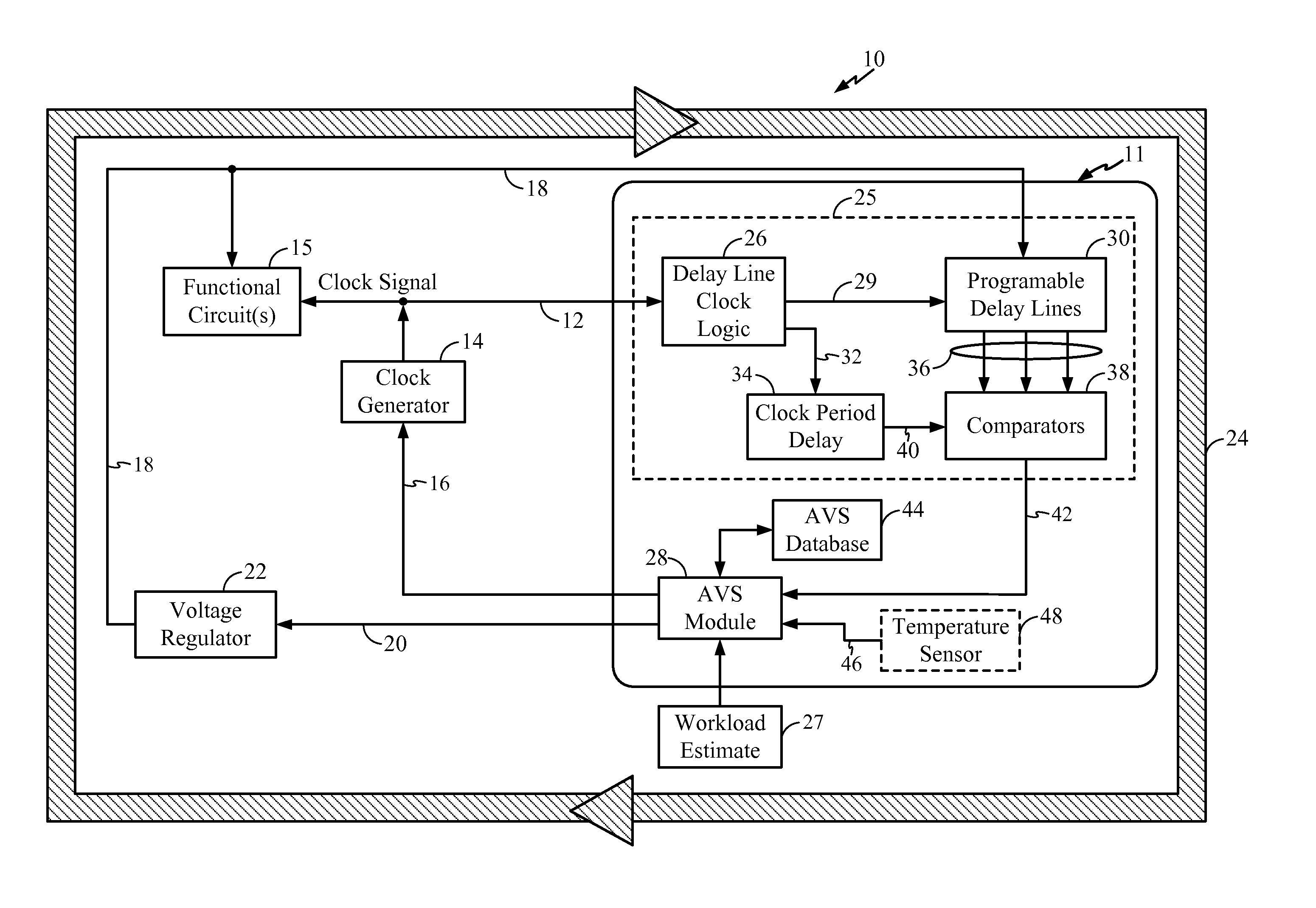
[0041]Embodiments disclosed in the detailed description include adaptive voltage scalers (AVSs), AVS systems, and related circuits and methods. The AVSs and AVS systems, circuits, and methods are configured to adaptively adjust the voltage level powering a functional circuit(s) based on a target or desired operating frequency and delay variation conditions for a functional circuit(s) to avoid or reduce voltage margin. Avoiding or reducing voltage margin can conserve power while maintaining proper functional circuit(s) operation. Delay variations can include one or more manufacturing variations specific to each AVS and functional circuit(s)...


PUM


Abstract

Adaptive voltage scalers (AVSs), systems, and related methods are disclosed. The AVSs are configured to adaptively adjust voltage levels powering a functional circuit(s) based on target operating frequencies and delay variation conditions to avoid or reduce voltage margin. In one embodiment, the AVS includes an AVS database. The AVS database can be configured to store voltage levels for various operating frequencies of a functional circuit(s) to avoid or reduce voltage margin. The AVS database allows rapid voltage level decisions. The voltage levels stored in the AVS database may be initial, minimum, learned, populated, explored, backed out, temperature-based, and / or age-based voltage levels according to disclosed embodiments to further avoid or reduce voltage margin. An AVS module may be a software-based module that consults the AVS database to make voltage level decisions. Providing the AVS module as a software-based module may allow flexibility in configuring the AVS module and / or the AVS database.

Description

RELATED APPLICATIONS[0001]The present application claims priority from and the benefit of U.S. Provisional Patent Application Ser. No. 61 / 164,882, filed Mar. 30, 2009, and U.S. Provisional Patent Application Ser. No. 61 / 222,779, filed Jul. 2, 2009, each of which is herein incorporated by reference in its entirety.BACKGROUND[0002]I. Field of the Disclosure[0003]The technology of the present application relates to adaptive voltage scalers (AVSs) and related systems for controlling the voltage level powering a circuit at a given operating frequency.[0004]II. Background[0005]Synchronous digital circuits, such as central processing units (CPUs) or digital signal processors (DSPs) as examples, require a clock signal to coordinate timing of logic in the circuit. The frequency of the clock signal controls the switching speed or rate of the logic and thus the performance of the circuit. There is a relationship between operating frequency and the voltage level. An increase in operating freque...

Claims


Application Information

Patent Timeline
Patent Type & Authority Patents(United States)
IPC IPC(8): G05F1/10G06F1/32
CPCG06F1/324G06F1/3296Y02B60/1285H03K3/012G06F1/3203G06F1/3234Y02B60/1217G05F1/462Y02D10/00G06F1/32G06F1/26G06F1/04
Inventor MOORE, RICHARD A.MICHALAK, GERALD PAULBRIDGES, JEFFREY T.
Owner QUALCOMM INC
Why Eureka
Try Eureka