

Apparatus for depositing a multilayer coating on discrete sheets
a multi-layer coating and apparatus technology, applied in the field of encapsulation tools, can solve the problems of increasing the complexity of design and control systems, difficult to deposit coatings onto rigid substrates or to substrates supporting inflexible devices mounted thereto, and maintaining vacuum adds considerable complexity, so as to reduce or eliminate the chance of interlayer contamination, the effect of maximizing the production rate of encapsulation and overall tool simplicity
- Summary
- Abstract
- Description
- Claims
- Application Information
AI Technical Summary
Benefits of technology
Problems solved by technology
Method used
Image

Examples
Embodiment Construction
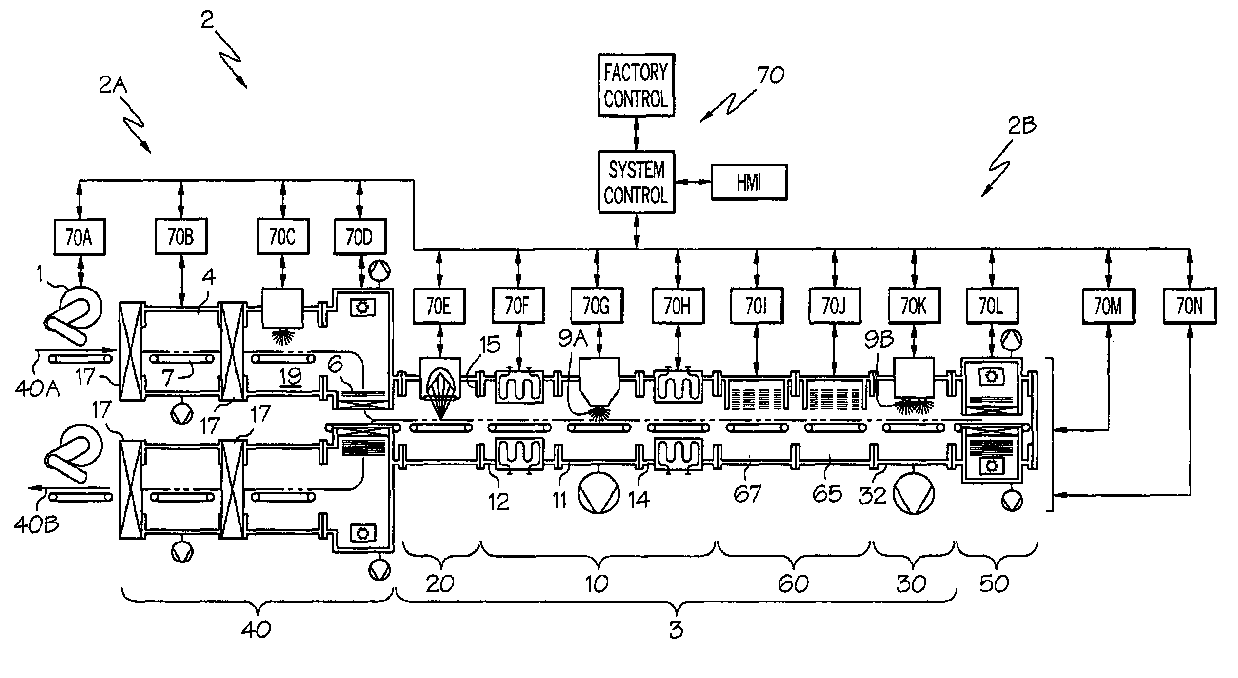
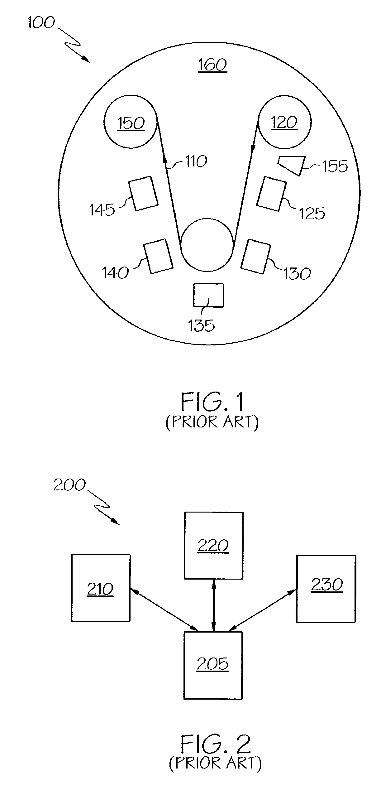
[0026]Referring first to FIG. 1, a roll-to-roll device 100 for depositing multilayer coatings on a continuous web of substrate according to the prior art is shown. A web of substrate 110 passes over a distribution reel 120 and past a first organic layer deposition station 125, curing station 130, inorganic layer deposition station 135, second organic layer deposition station 140 and curing station 145, and on to take-up reel 150. Optionally, the device 100 can include one or more surface treatment devices (such as plasma source 155) to improve the adhesion between the organic layer and the substrate 110. The interior of the device 100 defines a single chamber 160. A common vacuum is present among all of the aforementioned components. In one commonly used process, the polymer multilayer (PML) process, an organic precursor used at the first and second organic layer deposition stations 125 and 140 is flash evaporated such that when the organic precursor is introduced into the vacuum ch...
PUM
| Property | Measurement | Unit |
|---|---|---|
| temperature | aaaaa | aaaaa |
| energy | aaaaa | aaaaa |
| permeation resistance | aaaaa | aaaaa |
Abstract
Description
Claims
Application Information