Circuit module

a circuit module and circuit technology, applied in the direction of printed circuit non-printed electric components association, coupling device connection, fixed capacitor details, etc., can solve the problems of external received electrostatic noise, insufficient grounding, and inability to adequately ground,

Active Publication Date: 2014-08-19
MURATA MFG CO LTD
View PDF21 Cites 6 Cited by
  • Summary
  • Abstract
  • Description
  • Claims
  • Application Information

AI Technical Summary

Benefits of technology

[0016]At least two of the plurality of inner conductive layers directly connected to the shielding layer may be connected to each other through a conductive via in the substrate. In this case, the inner conductive layers have a uniform potential all over the inner conductive layers, and the resistivity of the inner conductive layers can be reduced.
[0021]As a result, a circuit module according to a preferred embodiment of the present invention can sufficiently ground electrostatic noise externally received by a shielding layer. An inner circuit is not therefore affected by the electrostatic noise. In addition, electrostatic noise generated in the inner circuit in the circuit module can be sufficiently grounded and is not externally transmitted.

Problems solved by technology

Accordingly, electrostatic noise externally received by the shielding layer 109 cannot be sufficiently grounded and an inner circuit may be affected by the electrostatic noise.
In addition, electrostatic noise generated by the inner circuit in the circuit module 300 cannot be sufficiently grounded, and the electrostatic noise may be externally transmitted.

Method used


Image

  • Circuit module
  • Circuit module
  • Circuit module

Examples


first preferred embodiment

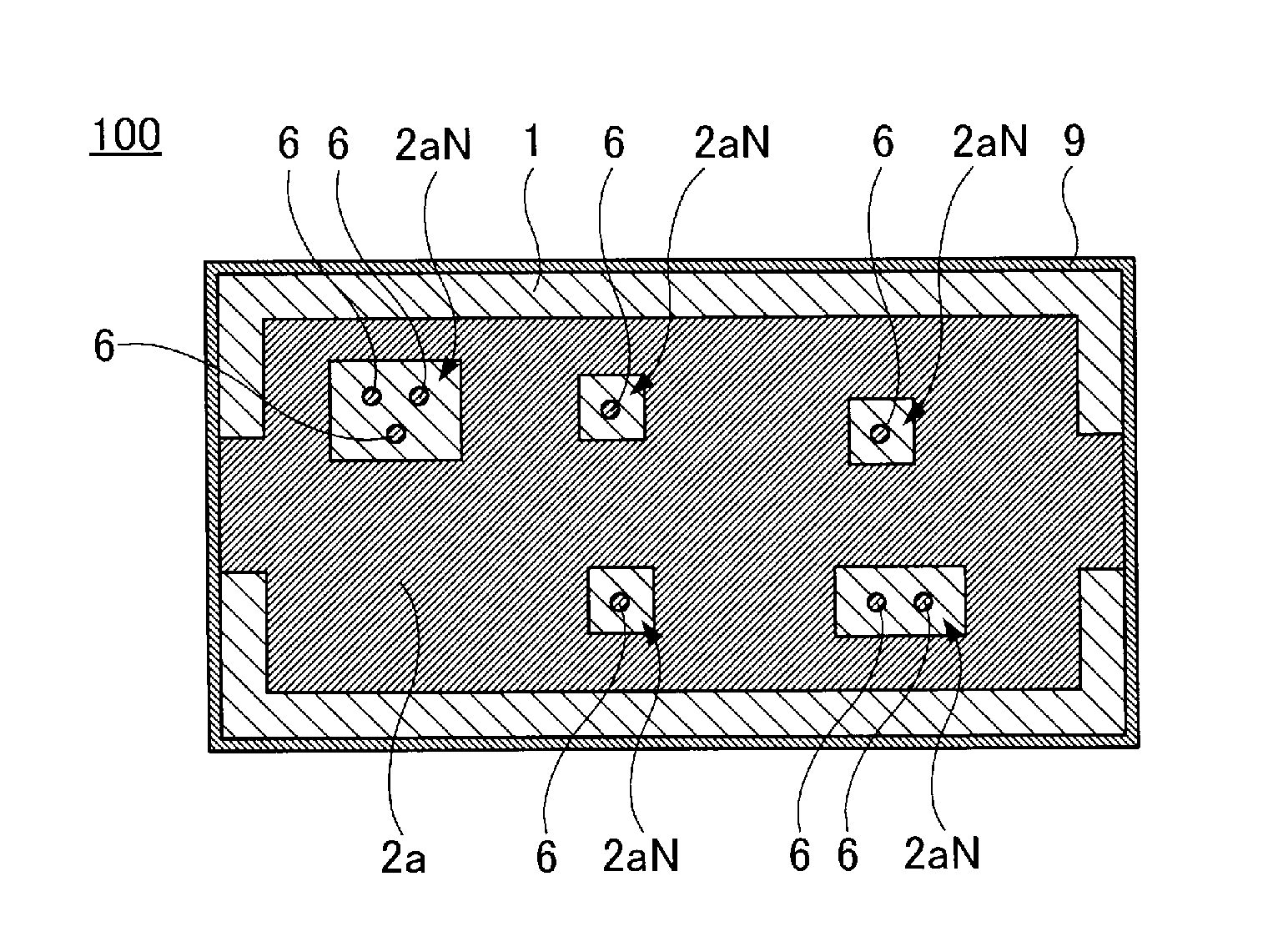
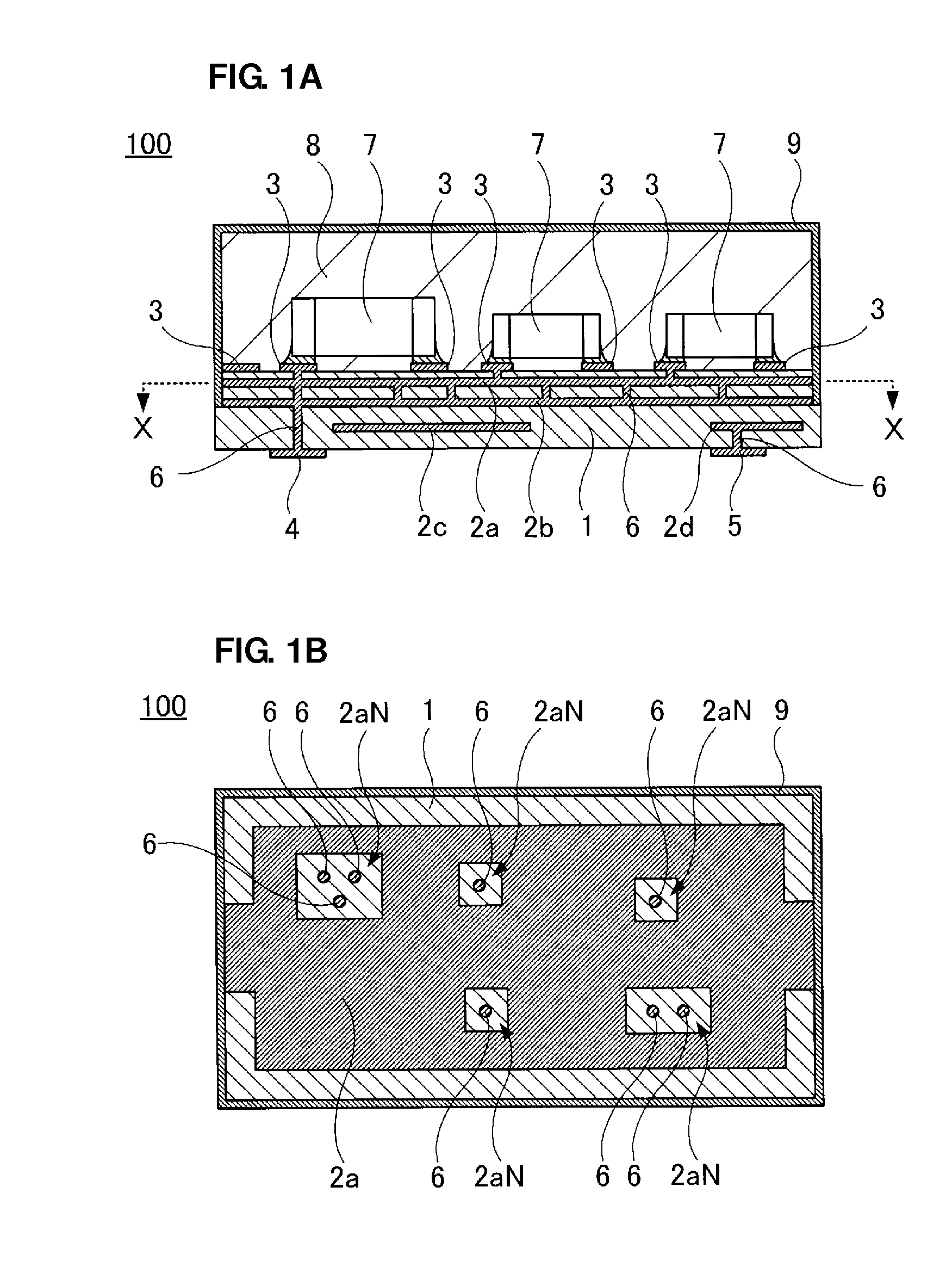
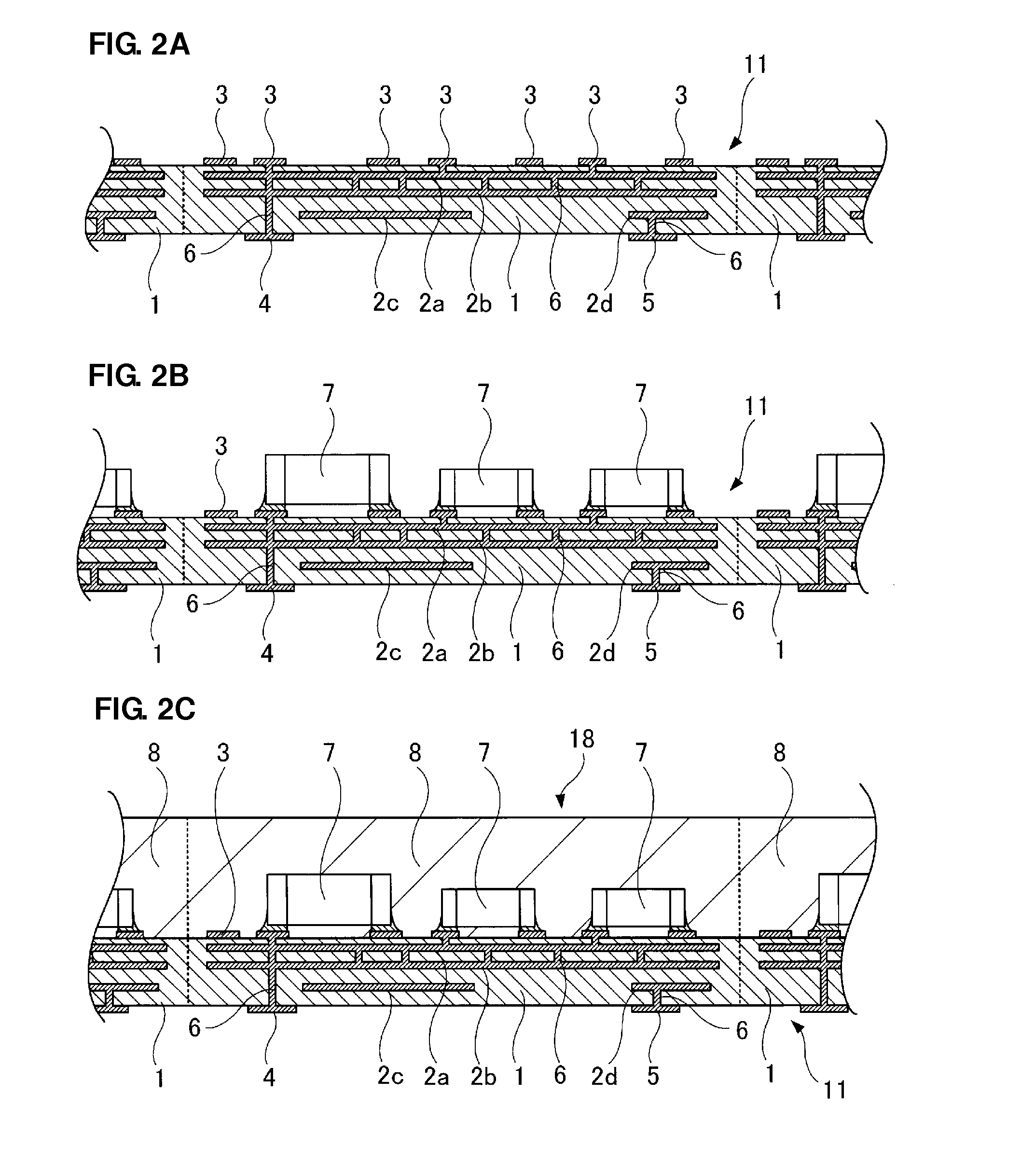
[0032]FIGS. 1A and 1B are diagrams illustrating a circuit module 100 according to the first preferred embodiment of the present invention. FIG. 1A is a cross-sectional view of the circuit module 100. FIG. 1B is a partial cross-sectional view of the circuit module 100 taken along a broken arrow X-X of FIG. 1A.

[0033]The circuit module 100 includes a substrate 1.

[0034]The substrate 1 may be made of any material, and can be made of, for example, low-temperature sintering ceramic containing the mixture of alumina and glass.

[0035]In the substrate 1, a plurality of inner conductive layers 2a, 2b, 2c, and 2d are disposed. On one main surface of the substrate 1, a plurality of land electrodes 3 are disposed. On the other main surface of the substrate 1, a ground electrode 4 and a terminal electrode 5 are disposed. In the substrate 1, a plurality of via electrodes 6 are disposed. Predetermined portions of the inner conductive layers 2a to 2d, the land electrodes 3, the ground electrode 4, and...

second preferred embodiment

[0058]A circuit module 200 according to the second preferred embodiment of the present invention is illustrated in FIG. 6. FIG. 6 is a cross-sectional view of the circuit module 200.

[0059]In the circuit module 200 according to the second preferred embodiment, on the mounting surface (the lower main surface illustrated in FIG. 1A) of the substrate 1 in the circuit module 100 according to the first preferred embodiment illustrated in FIGS. 1A and 1B, other electronic components are disposed and an additional insulating layer covering the other electronic components is provided.

[0060]That is, as illustrated in FIG. 6, in the circuit module 200, land electrodes 13 are disposed on the mounting surface of the substrate 1 in the circuit module 100. Electronic components 17 are mounted on the land electrodes 13. An insulating layer 28 is arranged so that it covers the electronic components 17. On the surface of the insulating layer 28, a ground electrode 14 and a terminal electrode 15 are d...


PUM


Abstract

A circuit module includes a substrate that has a substantially rectangular parallelepiped shape and includes a plurality of inner conductive layers, an electronic component disposed on a first main surface of the substrate, an insulating layer disposed on the first main surface of the substrate so as to cover the electronic component, a shielding layer disposed on a surface of the insulating layer, and a ground electrode connected to the plurality of inner conductive layers. At least two of the inner conductive layers are directly connected to the shielding layer.

Description

BACKGROUND OF THE INVENTION[0001]1. Field of the Invention[0002]The present invention relates to circuit modules, and, more particularly, to a circuit module in which a shielding layer disposed on a surface of an insulating layer covering an electronic component disposed on a substrate has a small thickness.[0003]2. Description of the Related Art[0004]In circuit modules in which an electronic component is disposed on a substrate and an insulating layer covers the electronic component, a shielding layer is sometimes formed on the surface of the insulating layer. Because of the shielding effect of the shielding layer, the electronic component disposed on the substrate is prevented from externally receiving electrostatic noise and failing to function normally, or is prevented from externally transmitting electrostatic noise.[0005]Japanese Unexamined Patent Application Publication No. 2004-172176 discloses such a circuit module. FIG. 7 is a diagram illustrating a circuit module 300 disc...

Claims


Application Information

Patent Timeline
Patent Type & Authority Patents(United States)
IPC IPC(8): H05K1/16H01L21/56H01L23/00H01L23/31H01L23/498H01L23/538H01L23/552H05K1/02H05K3/00H05K3/28
CPCH05K1/0218H01L21/561H01L23/3121H01L23/49822H01L23/5389H01L23/552H01L24/97H01L2224/16225H01L2224/48091H01L2224/48227H01L2224/97H01L2924/19105H01L2924/3025H05K3/0052H05K3/284H05K2201/0715H05K2203/1316H01L2924/00014H01L2224/81H01L2924/00
Inventor YOSHIDA, MASATO
Owner MURATA MFG CO LTD
Why Eureka
Try Eureka