
Semiconductor device and method for making the same using semiconductor fin density design rules

a technology of semiconductor fins and design rules, applied in the direction of cad circuit design, program control, instruments, etc., can solve the problems of destroying device functionality, difficult to control the profile of both types of fins, and the same limitations and shortcomings

Active Publication Date: 2014-08-19
TAIWAN SEMICON MFG CO LTD
View PDF50 Cites 9 Cited by
  • Summary
  • Abstract
  • Description
  • Claims
  • Application Information

AI Technical Summary

Benefits of technology

[0003]Another shortcoming associated with fins that are comparatively isolated, i.e. fins that are not in a densely packed feature environment, is the peeling phenomenon. Semiconductor fins that are comparatively isolated tend to peel and detach from the substrate upon which they are formed thereby destroying device functionality and contaminating the processing chamber in which the peeling occurs.

Problems solved by technology

When semiconductor fin devices are formed using patterning processes such as photolithography and etching, they are subject to the same limitations and shortcomings that are essentially inherent in such patterning processes such as the difference in size and profile between nested fins and isolated fins.
When isolated fins and groups of nested fins are formed simultaneously using the same patterning process, it is difficult to control the profiles of both types of fins and to produce the fins to have the same critical dimensions and profiles.
Semiconductor fins that are comparatively isolated tend to peel and detach from the substrate upon which they are formed thereby destroying device functionality and contaminating the processing chamber in which the peeling occurs.

Method used


Image

  • Semiconductor device and method for making the same using semiconductor fin density design rules
  • Semiconductor device and method for making the same using semiconductor fin density design rules
  • Semiconductor device and method for making the same using semiconductor fin density design rules

Examples


Embodiment Construction

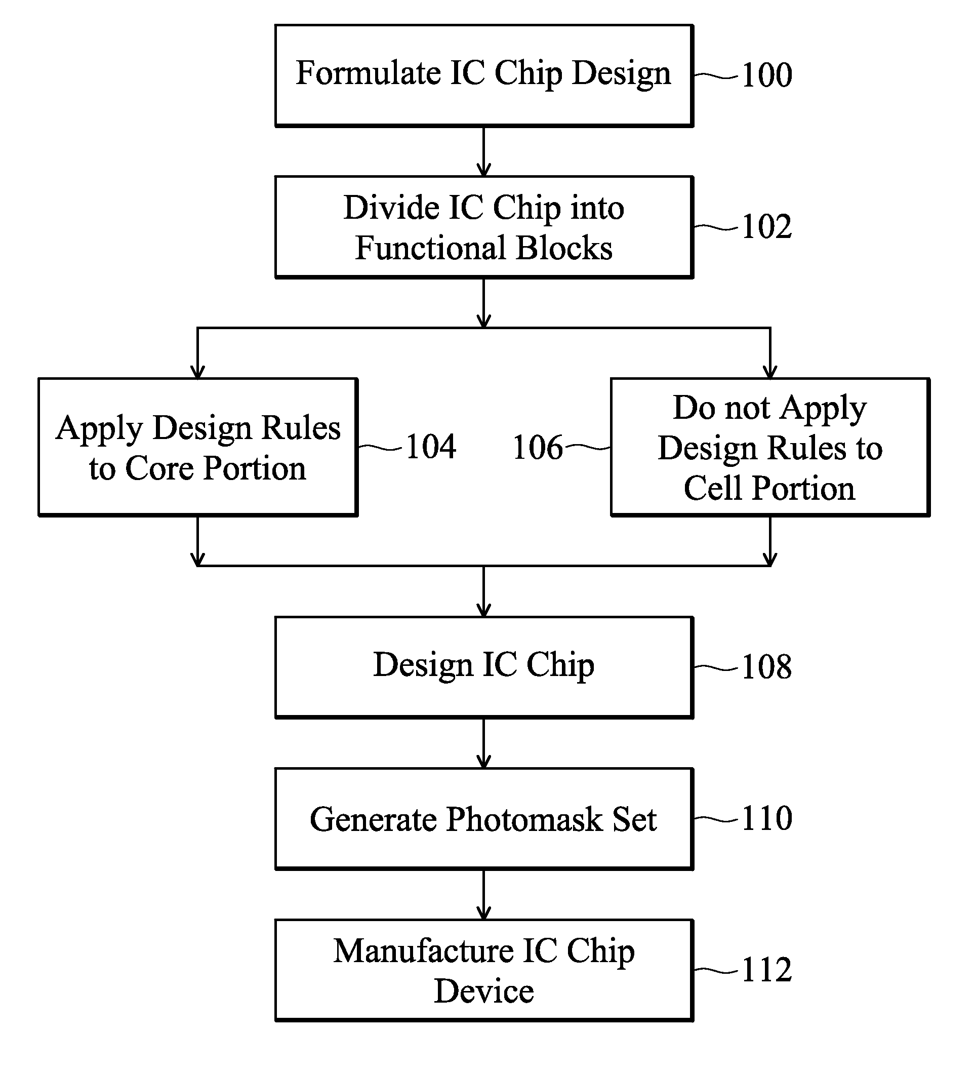
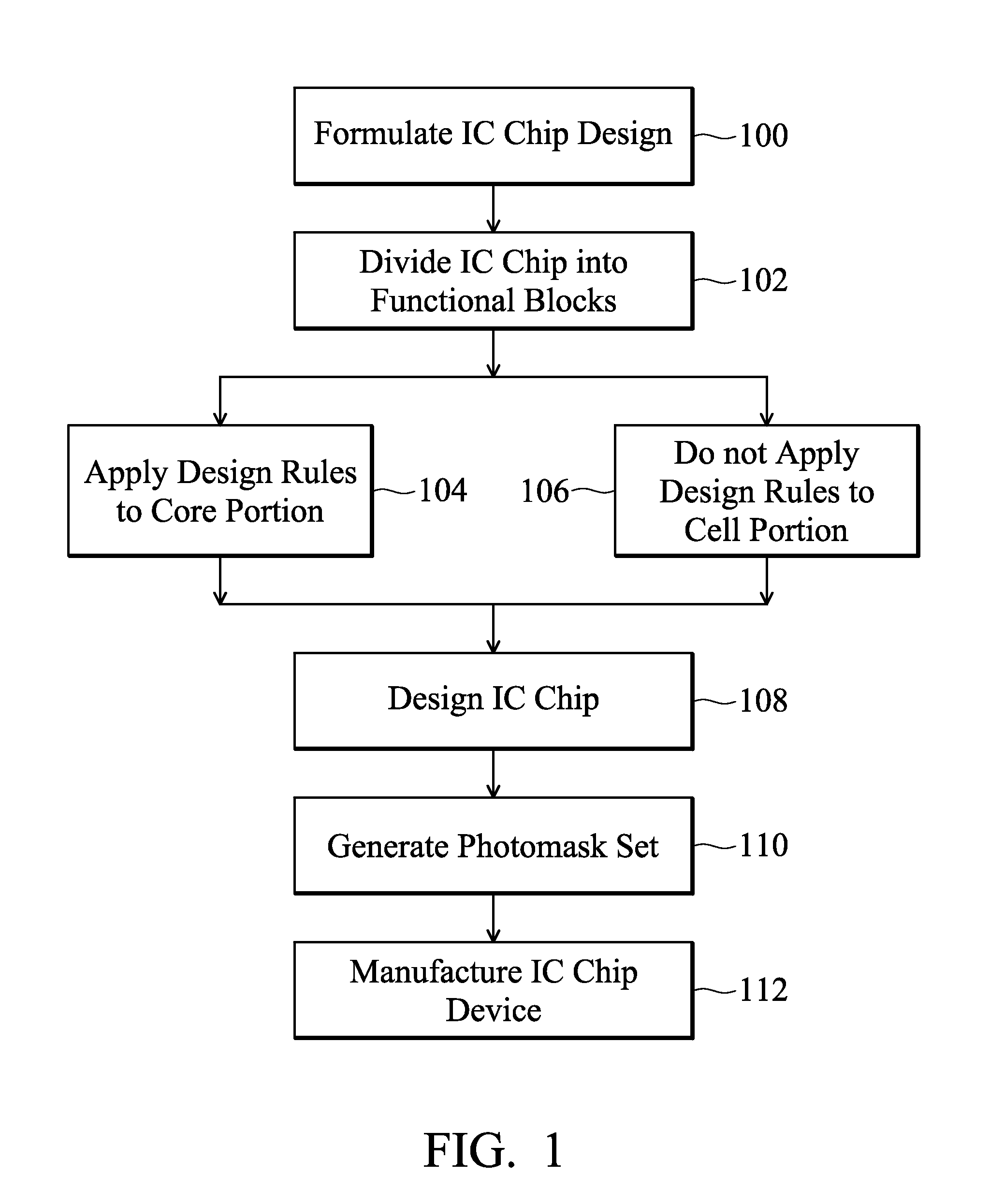
[0015]Aspects of the invention include a semiconductor device, a method for forming a semiconductor device, a method for designing a semiconductor device and a computer-readable medium having encoded thereon a computer-readable program code which, when executed, causes a computer to design the semiconductor device.

[0016]More particularly, the present invention provides a computer implemented or other method for semiconductor device design and for semiconductor device mask manufacturing based on the design. An aspect of the invention is a computer system such as a CAD (Computer Aided Design) system for carrying out the method by executing design steps and providing lithography data to generate a mask set. Various CAD systems are available and may be used. Design information is input to the CAD system and program instructions may be provided to the CAD system to enable the CAD system to design the mask set. Lithography data produced by the computer implemented design method may be pro...


PUM


Abstract

A method for designing a semiconductor ic chip includes dividing the chip into functional blocks such as a core portion and one or more other functional cells and applying design rules concerning the spatial arrangement of semiconductor fins to the core portion but not to the other functional cells. The design guidelines include the application of design rules to some but not all functional blocks of the chip, may be stored on a computer-readable medium and the design of the semiconductor ic chip and the generation of a photomask set for manufacturing the semiconductor ic chip may be carried out using a CAD or other automated design system. The semiconductor ic chip formed in accordance with this method includes semiconductor fins that are formed in both the core portion and the other functional cells but are only required to be tightly packed in the core portion.

Description

FIELD OF THE INVENTION[0001]The present invention relates, most generally, to semiconductor integrated circuits and methods for designing and manufacturing the same. More particularly, the present invention relates to manufacturing semiconductor integrated circuit devices according to design rules requiring semiconductor fins to be relatively tightly packed in core device sections whereas isolated semiconductor fins are allowed in more densely packed cells of the integrated circuit device.BACKGROUND[0002]Semiconductor fins are widely used in advanced semiconductor manufacturing technology because of the increased integration levels they provide. For example, when transistor devices such as FinFET, fin field effect transistor, devices are formed they provide a gate width that may be larger, by an order of magnitude, than the gate width of a transistor formed on the same substrate section in which the semiconductor fin is formed. Semiconductor fins have a high aspect ratio, i.e. they ...

Claims


Application Information

Patent Timeline
Patent Type & Authority Patents(United States)
IPC IPC(8): G06F9/455G06F17/50H01L21/20H01L27/12H01L29/66
CPCH01L27/1116G06F17/5072G06F2217/12H01L27/0207H01L27/105H01L29/785H01L27/11H10B10/18H10B10/00H01L21/823821H01L21/823431G06F30/392G06F30/39G06F2119/18H10B12/056
Inventor YU, SHAO-MINGCHANG, CHANG-YUN
Owner TAIWAN SEMICON MFG CO LTD
Learn More