

Apparatus for chip thermal stress relief
a chip and thermal stress technology, applied in electrical apparatus, semiconductor devices, semiconductor/solid-state device details, etc., can solve the problems of thermal expansion problem becoming even more important, the switching speed of semiconductor chips continues to increase, etc., to improve reliability and remove heat and thermal stress
- Summary
- Abstract
- Description
- Claims
- Application Information
AI Technical Summary
Benefits of technology
Problems solved by technology
Method used
Image

Examples
Embodiment Construction
[0028]The following description is presented to enable any person skilled in the art to make and use the disclosure, and is provided in the context of a particular application and its requirements. Various modifications to the disclosed embodiments will be readily apparent to those skilled in the art, and the general principle defined herein may be applied to other embodiments and applications without departing from the spirit and scope of the present disclosure. Thus, the present disclosure is not intended to be limited to the embodiments shown, but is to be accorded the widest scope consistent with the principle and features disclosed herein.
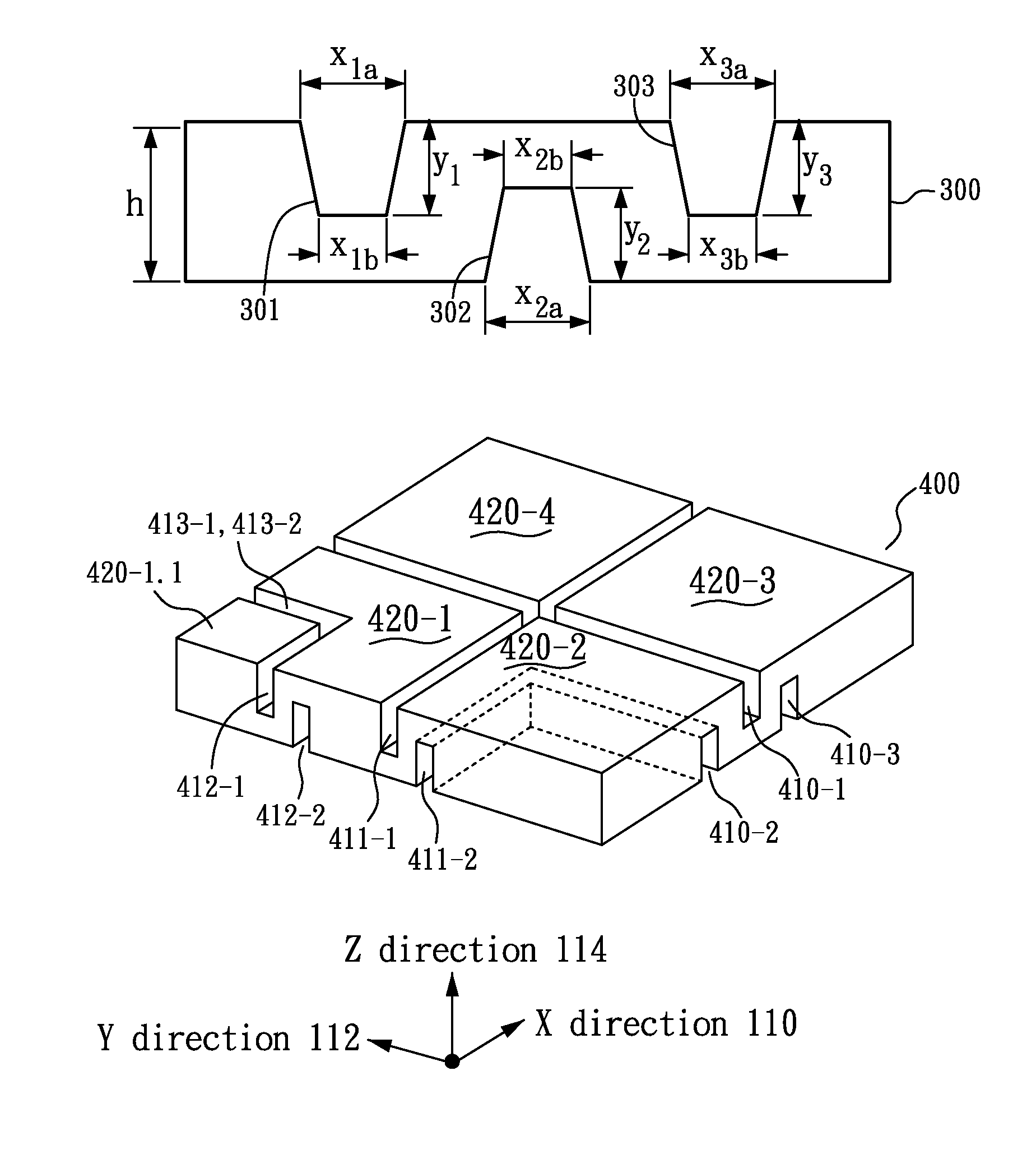
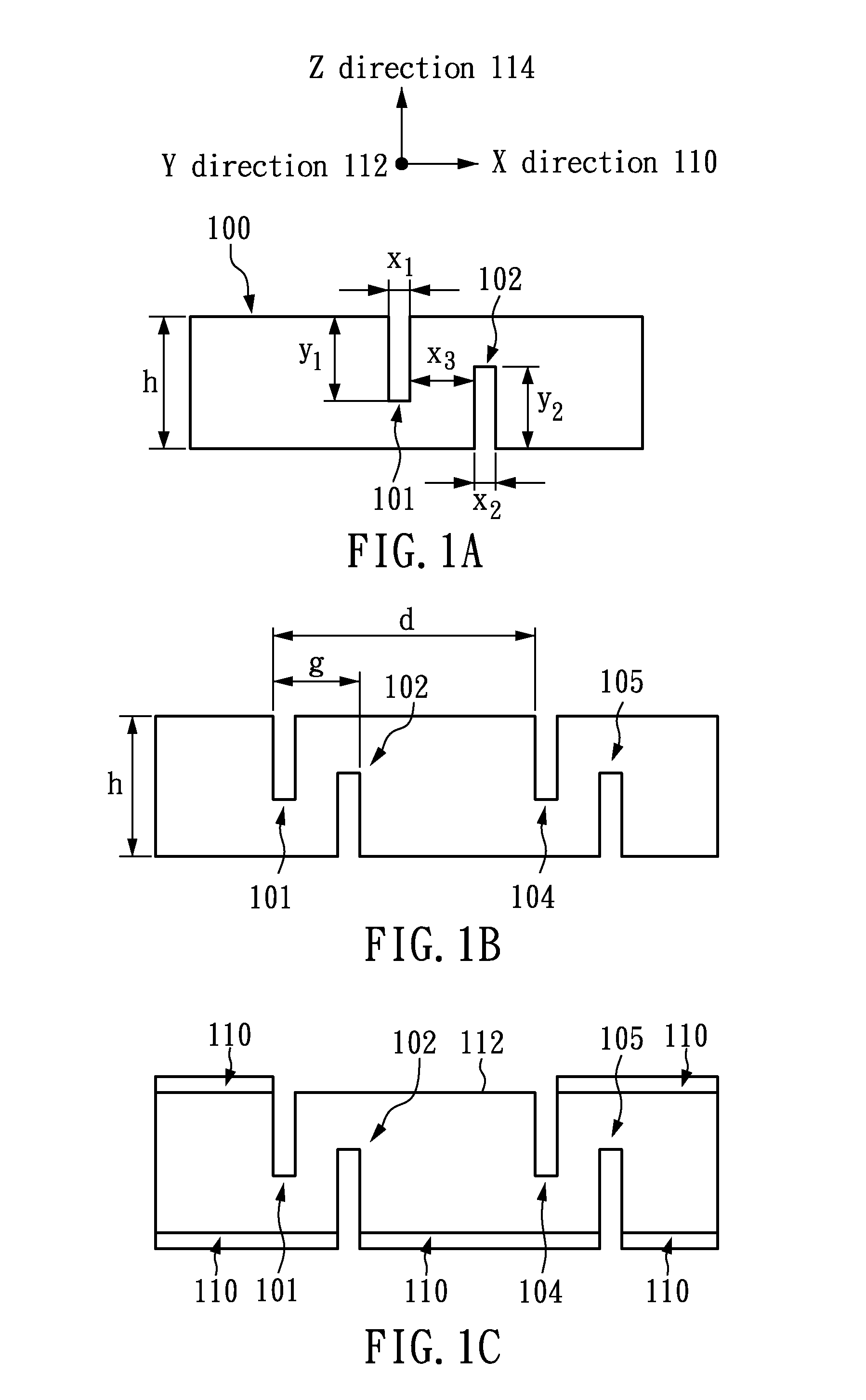
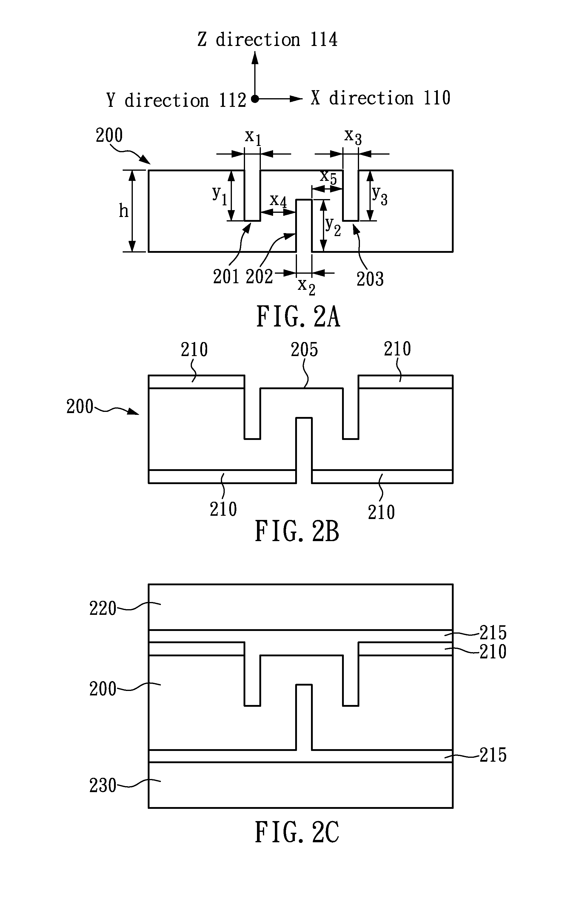
[0029]Due to mismatch of the thermal expansion coefficients of silicon chip (approximately 4.0E-6 / ° C.) and the package (e.g. Copper, approximately 16.5E-6 / ° C.), the stress generated from thermal expansion on silicon chips due to temperature changes (e.g. repetitive heating and cooling) usually causes chips to crack or even destroys the devic...
PUM
| Property | Measurement | Unit |
|---|---|---|
| thermal stress | aaaaa | aaaaa |
| thickness | aaaaa | aaaaa |
| distance | aaaaa | aaaaa |
Abstract
Description
Claims
Application Information