Bias circuit

a bias circuit and circuit technology, applied in the field of bias circuits, can solve the problems of unsuitable class c conventional current mirrors (like, etc.), and achieve the effects of reducing the need for bias circuit adjustment, reducing the need for impedance, and restricting the generation of undesirable memory effects and non-linearity

Active Publication Date: 2014-10-07
AMPLEON NETHERLANDS
View PDF10 Cites 3 Cited by
  • Summary
  • Abstract
  • Description
  • Claims
  • Application Information

AI Technical Summary

Benefits of technology

[0008]There is proposed a bias circuit that employs a transistor connected between the output of the bias circuit and a reference voltage (such as ground, for example). The transistor may be adapted to act as a non-linear load and may allow quick discharge of load capacitance in a switching mode. Thus, embodiments may provide fast thermal tracking and process compensation together with low video impedances. Embodiments may also be compact in size, exhibit lower power consumption, and provide a reduced switching time (such as below 100 ns for example). Embodiments may therefore be employed in MMIC's or discrete transistors, and will be suitable for Doherty amplifiers and Time Division (TD)) amplifiers.
[0015]Embodiments may exhibit low impedance to prevent parasitic modulation appearing at the output (e.g. at the input of a transistor to be biased), thus restricting the generation of undesirable memory effects and non-linearity. Embodiments may compensate for part-to-part variation in the threshold voltage of an amplifier's transistor, thus reducing a need for adjustment of the bias circuit.

Problems solved by technology

A conventional current mirror (like that shown in FIG. 1 for example) is therefore not suitable for Class C.

Method used


Image

  • Bias circuit
  • Bias circuit
  • Bias circuit

Examples


Embodiment Construction

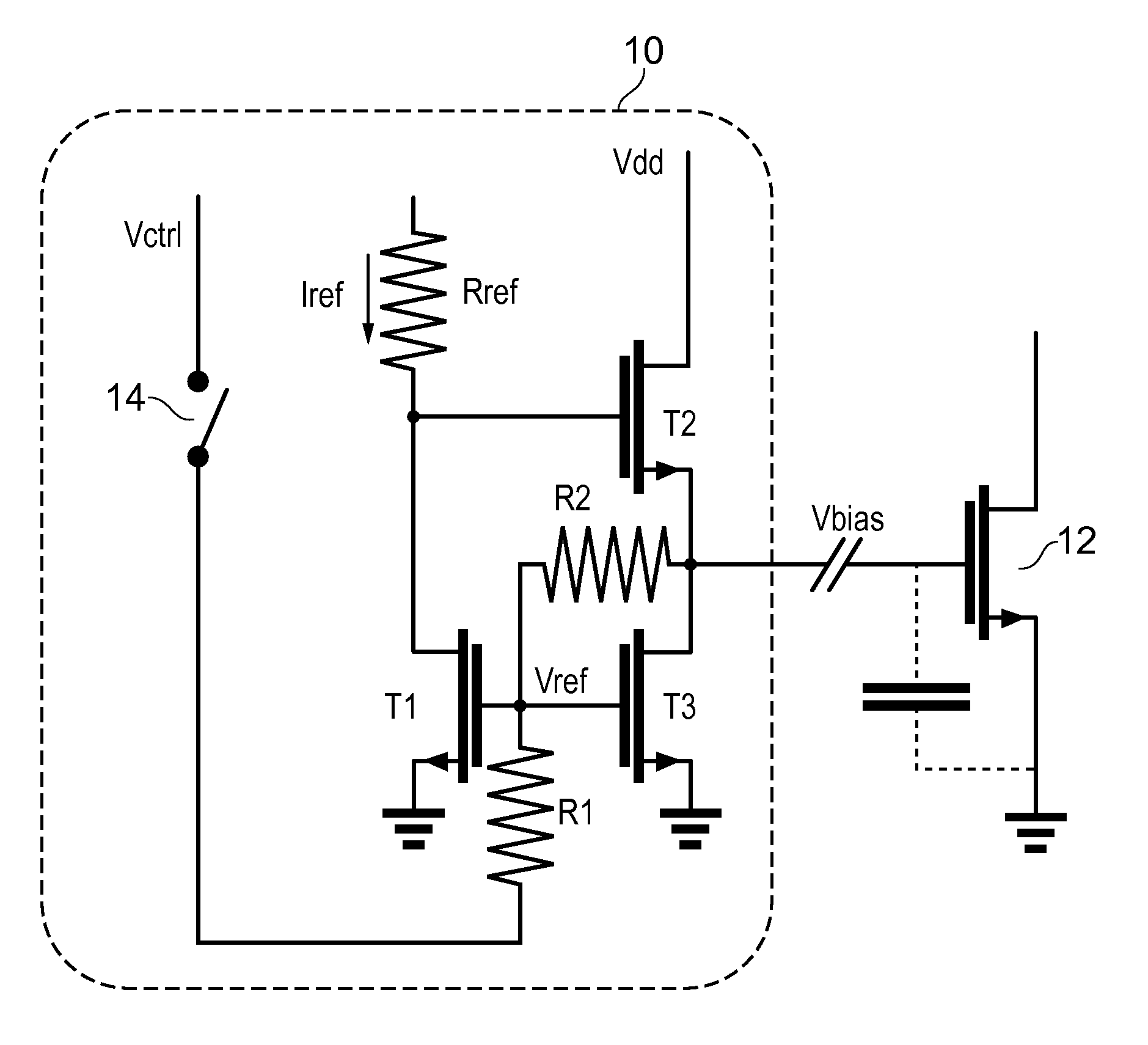
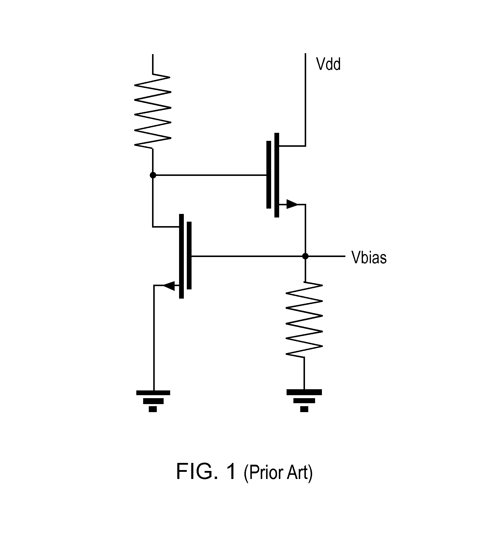
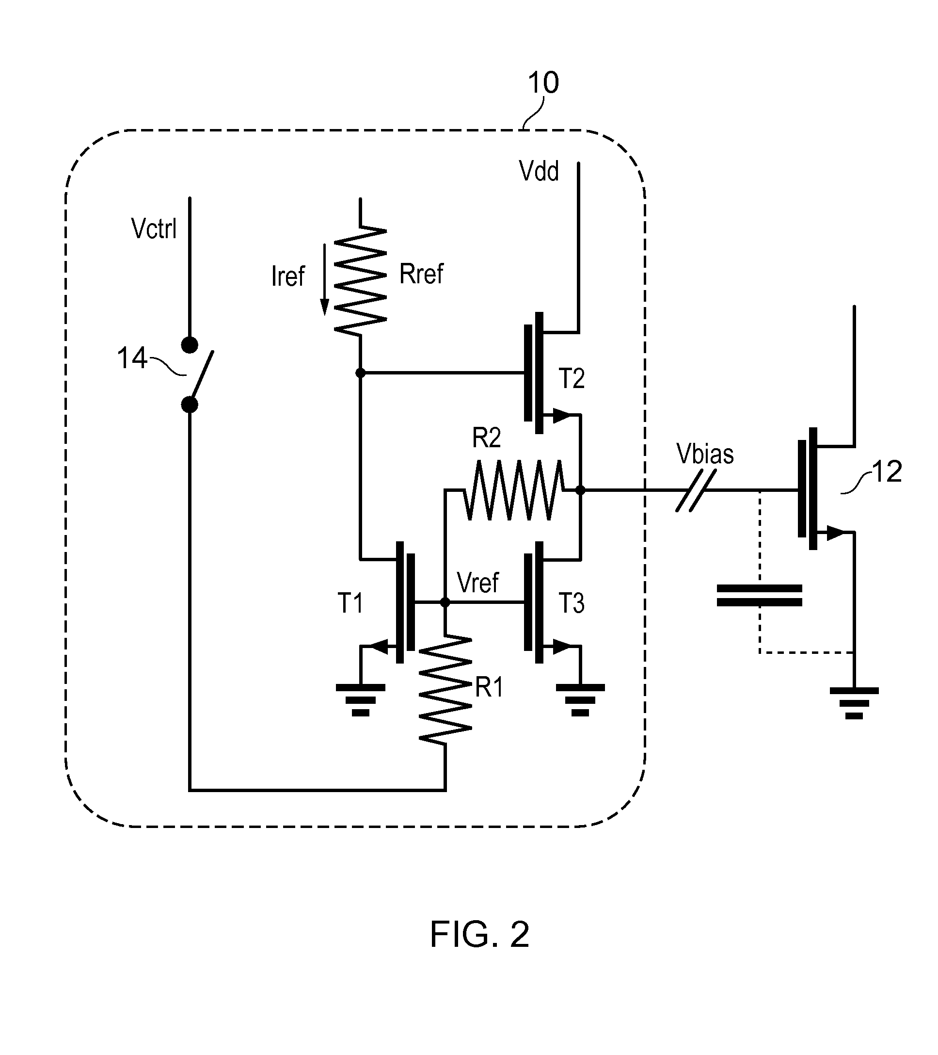
[0026]There is proposed a bias circuit which employs a current mirror circuit (similar to the conventional circuit arrangement shown in FIG. 1) to generate a bias voltage at an output terminal. The bias circuit also employs an additional transistor connected between the output terminal of the bias circuit and ground. This additional transistor can be controlled via a switch that is adapted to supply a control voltage to the control terminal (e.g. the gate) of the transistor.

[0027]An embodiment of a bias circuit 10 is shown in FIG. 2. The bias circuit 10 comprises first T1 and second T2 transistors which are scaled versions of a RF transistor T2 to be biased. The first T1 and second T2 transistors are provided in a looped arrangement, similar to that shown in FIG. 1, wherein the drain of the first transistor T1 is connected to a current source Iref. The voltage source Vdd is connected to the drain of the second transistor T2 and the gate of the second transistor T2 is connected to th...


PUM


Abstract

Proposed is a bias circuit for a transistor in a C class amplifier. The bias circuit comprises: a class AB amplifier bias voltage generating means adapted to generate a bias voltage at an output terminal; and a transistor connected between the output terminal and a first reference voltage, the control terminal of the transistor being connected to a second reference voltage via a switch. Closure of the switch connects the second reference voltage to the control terminal of the transistor to cause a shift in the bias voltage generated by the class AB amplifier bias voltage generating means to achieve a predetermined class C bias voltage at the output terminal.

Description

FIELD OF THE INVENTION[0001]This invention relates to a bias circuit for a Radio Frequency (RF) power transistor.CROSS-REFERENCE TO RELATED APPLICATIONS[0002]This application claims the priority under 35 U.S.C. §119 of European patent application no. 13290021.8, filed on Jan. 28, 2013, the contents of which are incorporated by reference herein.BACKGROUND OF THE INVENTION[0003]In the field of RF power amplification, with the increasing complexity of signals to be amplified (such as GSM, WCDMA, LTE, etc. . . . ) and the demand for efficiency, the preferred mode of operation of a RF transistor is a common source (emitter) class AB linear amplifier.[0004]In order to maintain linearity, it is known to use a bias circuit to provide thermal compensation. This has been implemented in MMIC's using the well-known current mirror arrangement of transistors. When integrated on the same die as a RF power transistor, this provides thermal tracking and process compensation.[0005]With the continued ...

Claims


Application Information

Patent Timeline
Patent Type & Authority Patents(United States)
IPC IPC(8): H03F3/04H03F1/02
CPCH03F1/0205H01L23/66H01L2223/665H01L2224/49175H01L2924/0002H03F1/0261H03F1/303H03F3/19H03F2200/18H01L2924/3011H01L2924/00
Inventor BOUNY, JEAN-JACQUES
Owner AMPLEON NETHERLANDS
Why Eureka
Try Eureka