Semiconductor die array structure

a technology of semiconductor integrated circuit and die array, which is applied in the direction of semiconductor/solid-state device details, electrical equipment, semiconductor devices, etc., can solve the problems of tool impact, die shift, die shift out of register, etc., and achieve the effect of reducing or substantially eliminating the shift of dies

Active Publication Date: 2014-11-11
INVENSAS CORP
View PDF262 Cites 2 Cited by
  • Summary
  • Abstract
  • Description
  • Claims
  • Application Information

AI Technical Summary

Benefits of technology

[0013]According to the invention, die shift is reduced or substantially eliminated, by cutting the wafer in two stages. In some embodiments a first wafer cutting procedure is carried out ...

Problems solved by technology

However, some procedures for preparing die require access to die sidewalls.
In particular, movement of the dicing saw during the wafer cutting procedure may cause die to shift out of register.
Out-of-register die can present challenges for subsequent preparation of the die in the array.
For example, die shift may result in a narrowing of the spaces between the die in the array, so that the streets are narrowed at some places, or are not straight.
Where a subsequent die preparation procedure calls for an additional pass of a cutting tool through the street,...

Method used


Image

  • Semiconductor die array structure
  • Semiconductor die array structure
  • Semiconductor die array structure

Examples


Embodiment Construction

[0035]The invention will now be described in further detail by reference to the drawings, which illustrate alternative embodiments of the invention. The drawings are diagrammatic, showing features of the invention and their relation to other features and structures, and are not made to scale. For improved clarity of presentation, in the FIGs. illustrating embodiments of the invention, elements corresponding to elements shown in other drawings are not all particularly renumbered, although they are all readily identifiable in all the FIGs. Also for clarity of presentation certain features are not shown in the FIGs., where not necessary for an understanding of the invention. For example, details of the circuitry within the die are omitted.

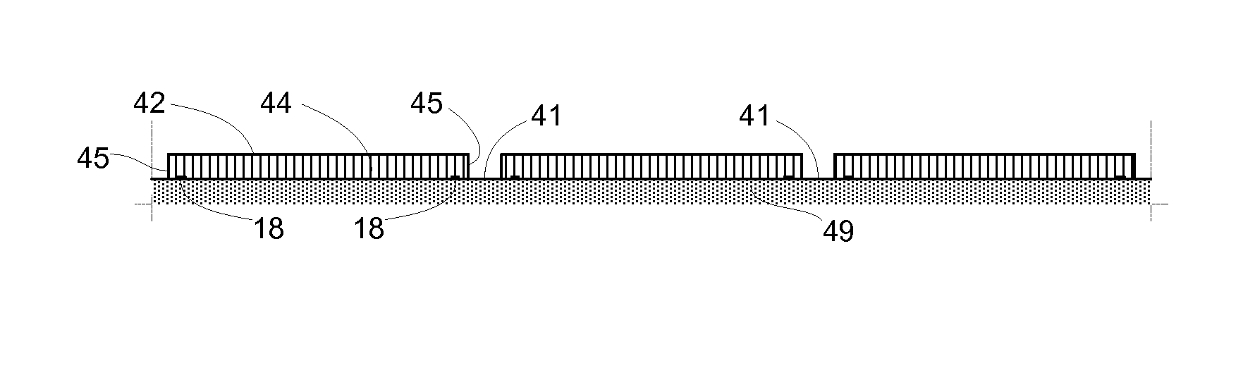
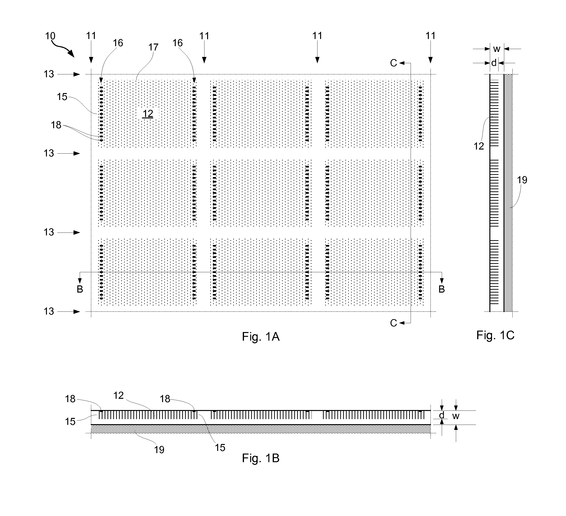
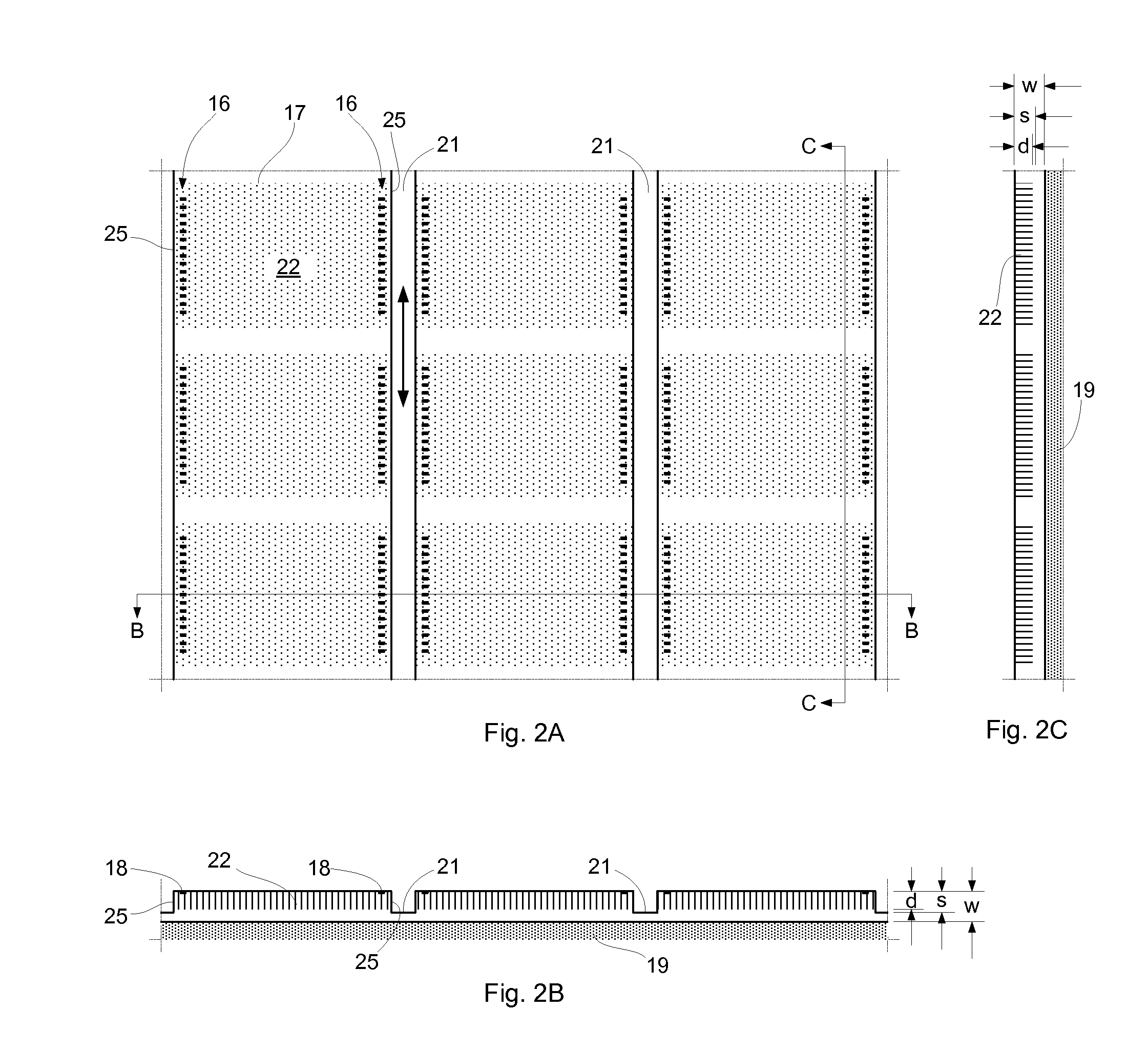
[0036]Turning now to FIG. 12, there is shown in a diagrammatic plan view a portion of a semiconductor wafer 120, such as a silicon wafer, with the active side in view. A number of integrated circuit chips are formed on the wafer, one of which is indic...


PUM


Abstract

According to the invention, die shift is reduced or substantially eliminated, by cutting the wafer in two stages. In some embodiments a first wafer cutting procedure is carried out prior to thinning the wafer to the prescribed die thickness; and in other embodiments the wafer is thinned to the prescribed die thickness prior to carrying out a first wafer cutting procedure. The first wafer cutting procedure includes cutting along a first set of streets to a depth greater than the prescribed die thickness and optionally along a second set of streets to a depth less than the die thickness. The result of the first cutting procedure is an array of strips or blocks of die, each including a plurality of connected die, that are less subject to shift than are individual singulated die. In a second wafer cutting procedure the die are singulated by cutting through along the second set of streets. Subsequent to the first cutting procedure, and prior to the second cutting procedure, additional die preparation procedures that are sensitive to die shift may be carried out.

Description

CROSS-REFERENCE TO RELATED APPLICATIONS[0001]This application is a Divisional of R. Co et al. U.S. Application Ser. No. 12 / 323,288, which was filed Nov. 25, 2008 and is now U.S. Pat. No. 7,863,159.[0002]The said U.S. application Ser. No. 12 / 323,288 claims the benefit of the filing date of R. Co et al. U.S. Provisional Application No. 61 / 132,708, titled “Semiconductor die separation method”, which was filed Jun. 19, 2008.[0003]This application is related to S.J.S. McElrea et al. U.S. application Ser. No. 12 / 142,589, which was filed 10 Jun. 19, 2008 and which is now U.S. Pat. No. 7,923,349. The above-referenced applications are hereby incorporated herein by reference.BACKGROUND OF THE INVENTION[0004]This invention relates to semiconductor wafer processing and, particularly, to preparing singulated semiconductor integrated circuit die.[0005]At some stage in die preparation, the wafer is cut to singulate the die. That is, the wafer is cut (for example, by sawing the wafer along “streets...

Claims


Application Information

Patent Timeline
IPC IPC(8): H01L21/78H01L21/683H01L23/00H01L23/544
CPCH01L2221/68359H01L2221/6834H01L21/6836H01L24/83H01L21/6835H01L2221/68327H01L24/27H01L21/78H01L2224/83191H01L2224/274H01L2924/1461H01L2924/14H01L2924/00
Inventor CO, REYNALDOMELCHER, DEANN EILEENPAN, WEIPINGVILLAVICENCIO, GRANT
Owner INVENSAS CORP
Why Eureka
Try Eureka