Optical waveguide structure and optical waveguide device

a technology of optical waveguides and optical waveguides, applied in optical waveguide light guides, instruments, optics, etc., can solve the problems of difficult to reduce the size of the device, difficult to manufacture, and difficult to couple light propagating through optical fibers or thorough spaces with optical waveguide devices using silicon platforms, etc., to achieve high efficiency and reduce conversion loss

Active Publication Date: 2014-12-16
NEC CORP
View PDF8 Cites 14 Cited by
  • Summary
  • Abstract
  • Description
  • Claims
  • Application Information

AI Technical Summary

Benefits of technology

[0028]According to the present invention, it is possible to provide a small optical waveguide structure capable of converting the spot size of light, and capable of reducing the conversion loss when compared under the condition of the same waveguide length and performing an optical conversion with high efficiency.

Problems solved by technology

However, it is believed that it is difficult to couple light propagating through an optical fiber or thorough space with an optical waveguide device using a silicon platform.
In the case of the latter devices (2), it is necessary to increase the taper length of the inverse taper section and the length of the upper clad section to several hundred μm or longer, and thus it is very difficult to reduce the devices in size.
However, its manufacturing process is complicated, and thus making the manufacturing very difficult.

Method used


Image

  • Optical waveguide structure and optical waveguide device
  • Optical waveguide structure and optical waveguide device
  • Optical waveguide structure and optical waveguide device

Examples


first exemplary embodiment

[0047]An optical waveguide structure and a configuration of an optical waveguide device including this optical waveguide structure according to an exemplary embodiment in accordance with the present invention are explained with reference to the drawings.

[0048]FIG. 1A is a perspective view of the main part of an optical waveguide device according to this exemplary embodiment. Further, FIG. 1B is a top view of the main part and FIG. 1C is a side view of the main part. To make the drawings to be viewed more easily, the scale and the position of each component are changed as appropriate from the actual scale and position and the illustration of some components is omitted in the drawings. Hatching is also omitted as appropriate in the cross sections.

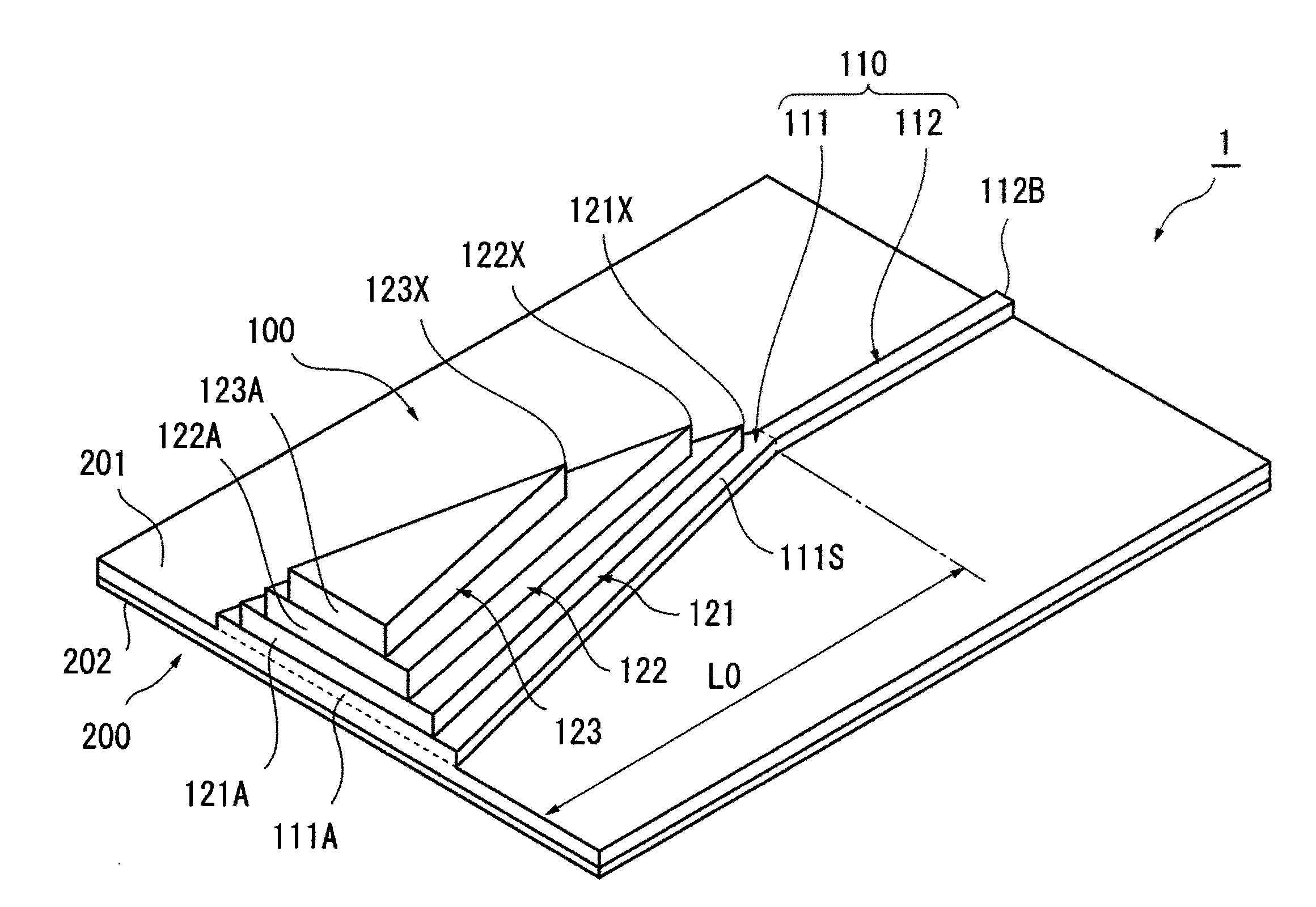
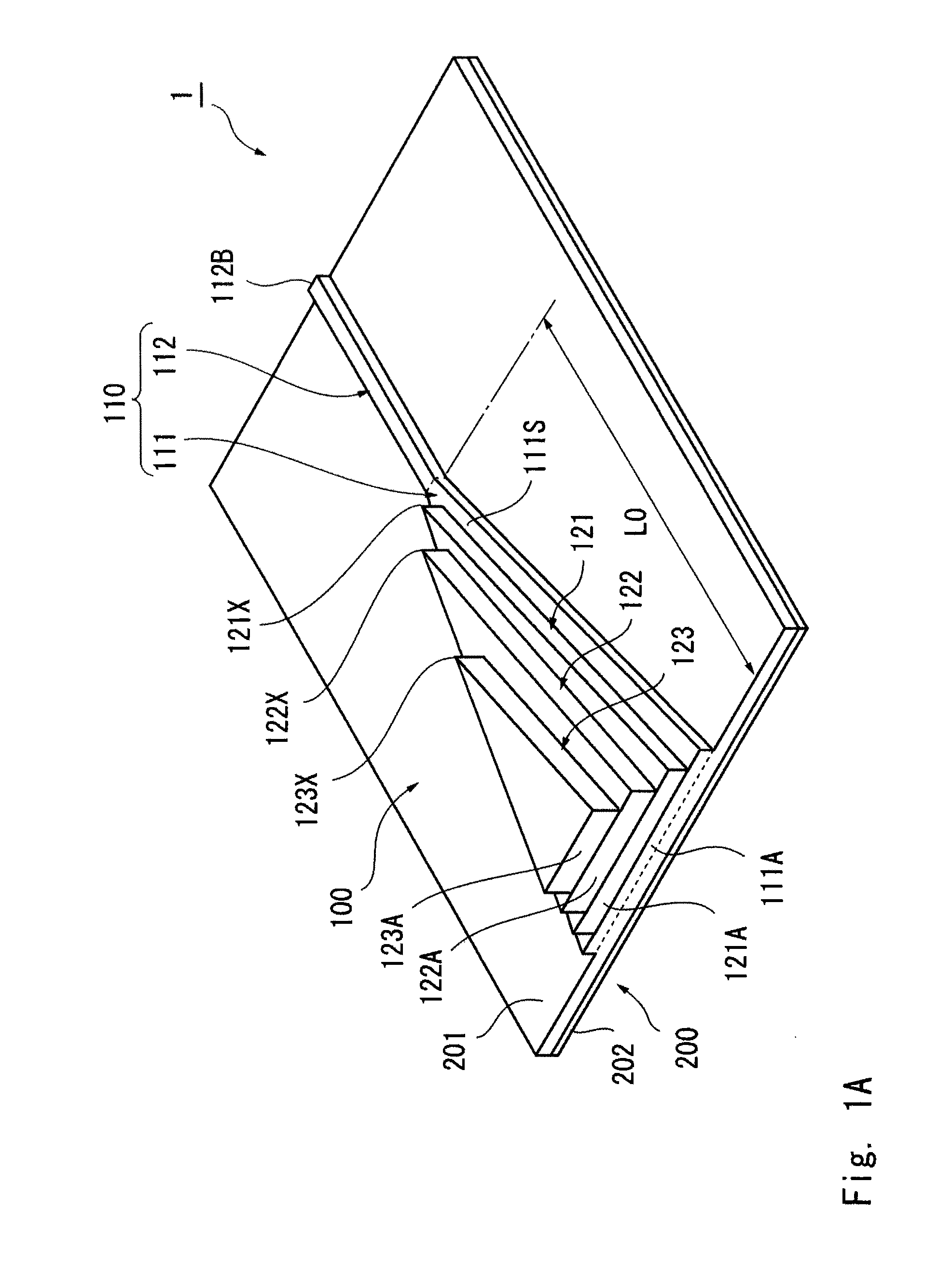
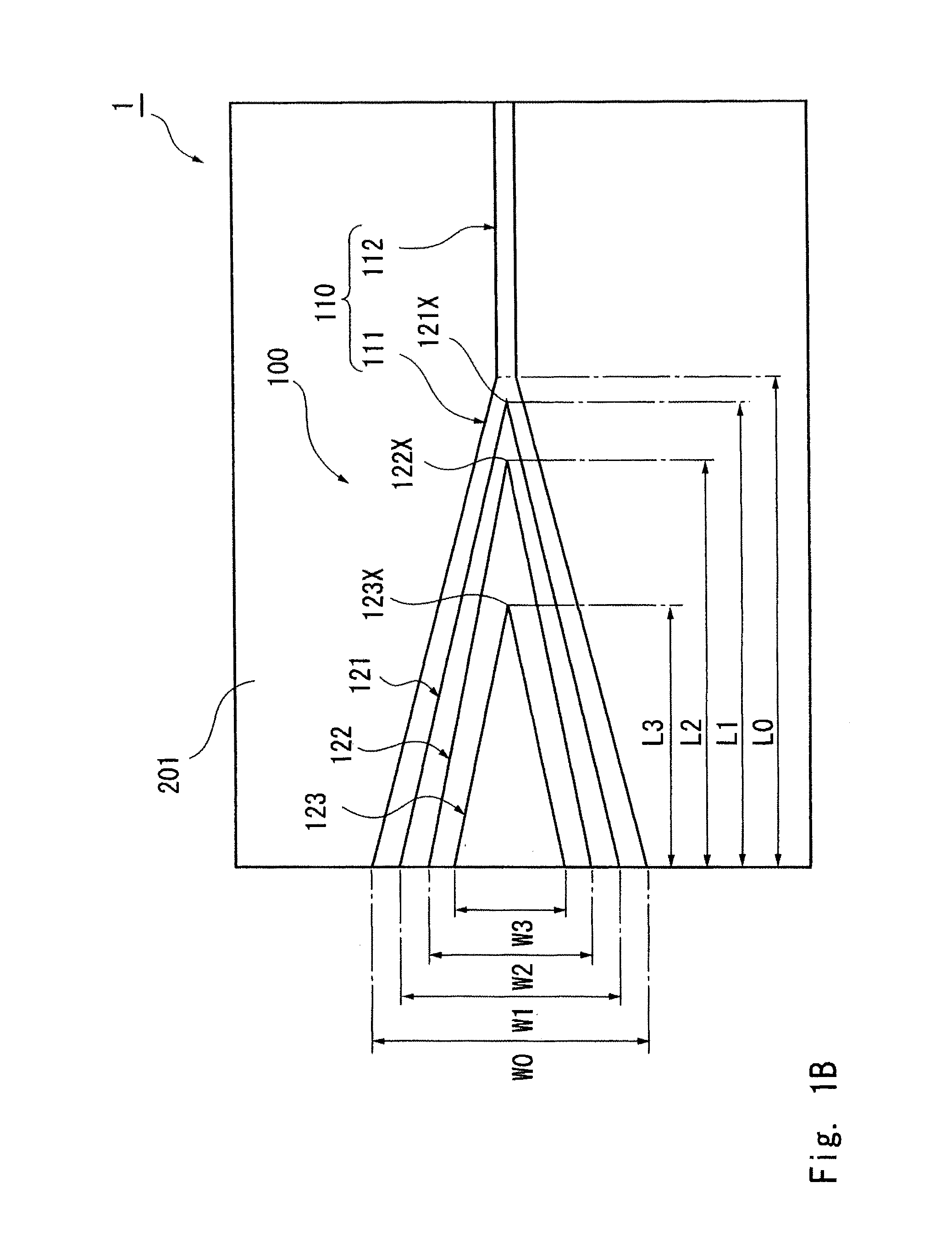
[0049]An optical waveguide device 1 according to this exemplary embodiment is a device in which an optical waveguide structure 100 is formed on an SOI (Silicon on Insulator) substrate 200.

[0050]For the SOI substrate 200, only the main part lo...

example 1

[0115]Calculation of an optical loss was carried out for an optical waveguide device including a base waveguide 110 and three-layered wedge-shaped upper waveguides 121 to 123 stacked above the base waveguide 110 like the one shown in FIGS. 1A to 1C. In this optical waveguide device, the relations “W0>W1>W2>W3” and “L0>L1>L2>L3” are satisfied.

(Note that,

Taper section 111 of base waveguide 110: Maximum width W0, Waveguide length L0;

Upper waveguide 121: Maximum width W1, Waveguide length L1;

Upper waveguide 122: Maximum width W2, Waveguide length L2; and

Upper waveguide 123: Maximum width W3, Waveguide length L3.)

[0116]As shown in FIG. 2A, the device is configured in such a manner that when the upper surface 111S of the taper section 111 of the base waveguide 110 is defined as a reference surface, as viewed from the side, the cusps of tips 121X to 123X of the upper waveguides 121 to 123 are connected with each other on a straight line.

[0117]The distance C1 between the cusp of tip 121X of...

examples 2-1 to 2-3

[0122]In Examples 2-1 to 2-3, calculation was carried out in a similar manner to that of Example 1 except that the positions of the cusps of tips 121X to 123X of the upper waveguides 121 to 123 were changed.


PUM


Abstract

The present invention provides a small optical waveguide structure capable of converting the spot size of light, and capable of reducing the conversion loss when compared under the condition of the same waveguide length and performing an optical conversion with high efficiency. An optical waveguide structure (100) includes a base waveguide (110) including a taper section (111) whose width becomes continuously narrower from one side toward another side, and a narrow-width section (112) that is consecutively connected to a narrow-width side of the taper section (111) and extends toward the another side. In the optical waveguide structure (100), at least three-layered upper waveguides (121 to 123) each of which has a planar shape smaller than the taper section (111) and includes a planar-view-roughly-wedge-shaped section whose width becomes continuously narrower from the one side toward the another side at least on a tip side are stacked above the taper section (111) of the base waveguide (110) in such a manner that the planar shape becomes successively smaller from the base waveguide side (110).

Description

[0001]This application is the National Phase of PCT / JP2011 / 005319, filed Sep. 21, 2011, which claims priority to Japanese Application No. 2010-217468, filed Sep. 28, 2010, and PCT application No. PCT / JP2011 / 003504, filed on Jun. 20, 2011, the disclosures of which are incorporated herein in their entireties by reference.TECHNICAL FIELD[0002]The present invention relates to an optical waveguide structure and an optical waveguide device.BACKGROUND ART[0003]Information communication networks typified by the Internet are spread all over the world as the infrastructure indispensable to people's lives. As a technique that supports the traffic of this Internet, there is an optical communication technology using optical fibers. Optical communication devices using a silicon platform capable of using 1.3 μm band and 1.5 μm band among the optical fiber communication wavelength bands have been expected as communication devices capable of realizing high-density optical integrated circuits that ca...

Claims


Application Information

Patent Timeline
Patent Type & Authority Patents(United States)
IPC IPC(8): G02B6/30G02B6/10G02B6/122G02B6/26
CPCG02B6/26G02B6/1228G02B6/305
Inventor USHIDA, JUNNAKAMURA, SHIGERU
Owner NEC CORP
Why Eureka
Try Eureka