Semiconductor drive circuit and power conversion apparatus using same

a technology of drive circuit and power conversion apparatus, which is applied in the direction of pulse generator, pulse technique, instruments, etc., can solve the problems of difficult to stably secure the dead time, increase parasitic capacitance inside the device, and turn on action of junction fet, so as to increase the turn-off speed, the effect of increasing the turn-on time and ensuring the dead tim

Inactive Publication Date: 2015-01-06
HITACHI LTD
View PDF17 Cites 5 Cited by
  • Summary
  • Abstract
  • Description
  • Claims
  • Application Information

AI Technical Summary

Benefits of technology

[0020]According to the present invention, in a semiconductor drive circuit for driving switching devices of a wide band gap semiconductor, the dead time can be secured stably through the reduction of the turn-off time (increase of the turn-off speed) and the relaxation (increase) of the turn-on time.
[0021]According to an embodiment of the present invention, both the securement of the dead time and low conduction loss can be achieved in a semiconductor drive circuit for driving switching devices of a wide band gap semiconductor such as SiC-JFETs.
[0022]According to an embodiment of the present invention, both the securement of the dead time and the low conduction loss can be achieved in a power conversion apparatus employing switching devices using a wide band gap semiconductor, in a power supply circuit employing such a power conversion apparatus, and in a motor driving circuit employing such a power conversion apparatus.
[0023]According to an embodiment of the present invention, miniaturization and high efficiency of the apparatus can be achieved through the reduction of the conduction loss.

Problems solved by technology

On the other hand, the reduction in the semiconductor layer thickness shortens the distances between the source / drain / gate electrodes and is causing an increase in parasitic capacitance inside the device (gate-drain capacitance (Cgd), gate-source capacitance (Cgs), drain-source capacitance (Cds)).
However, trouble occurs when the voltage between the terminals of the pulse transformer changes from −Vts [V] to 0 [V] in a state in which electric potential making the gate's side of the capacitor 15a be the positive side is remaining at the terminals of the capacitor 15a due to a factor like a too short OFF period.
In this state, due to the application of the voltage via the capacitor 15a, positive voltage is applied between the gate and the source of the junction FET, causing the turn ON action of the junction FET and making it difficult to stably secure the dead time.
Therefore, since the gate-source voltage of the switching element cannot be set negative at the time of turning OFF and the reduction of the turn-off time (increase of the turn-off speed) is impossible, it has been difficult to stably secure the dead time.

Method used


Image

  • Semiconductor drive circuit and power conversion apparatus using same
  • Semiconductor drive circuit and power conversion apparatus using same
  • Semiconductor drive circuit and power conversion apparatus using same

Examples


example 1

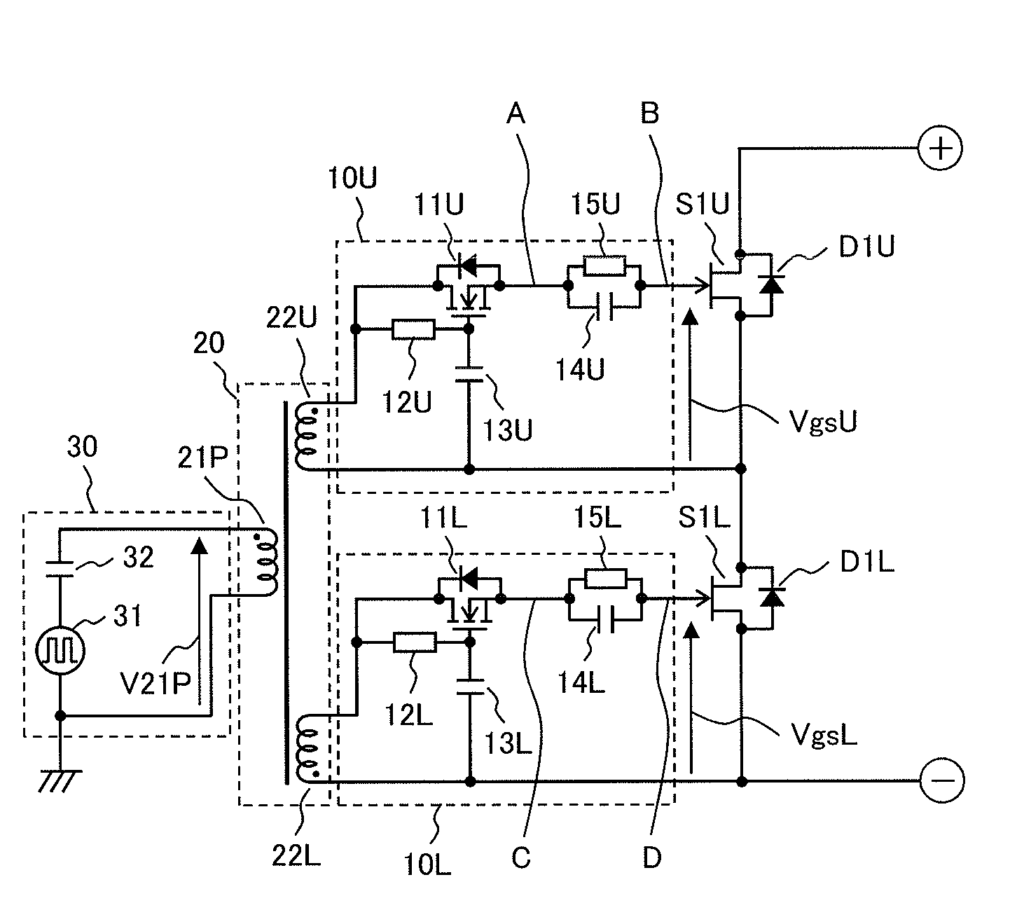
[0030]FIG. 1 is a circuitry diagram of a semiconductor drive circuit in accordance with a first embodiment of the present invention. FIG. 1 shows a part of the semiconductor drive circuit regarding switching devices for one phase (upper and lower arms connected in series).

[0031]Among the switching devices for one phase (upper and lower arms connected in series) shown in FIG. 1, the upper arm is made up of a normally-OFF junction FET S1U using SiC (SiC-JFET) and a Schottky barrier diode D1U using SiC (SiC-SBD), for example. Similarly, the lower arm is made up of a normally-OFF junction FET S1L using SiC (SiC-JFET) and a Schottky barrier diode D1L using SiC (SiC-SBD).

[0032]In the following explanation, the junction FETs S1U and S1L and the Schottky barrier diodes D1U and D1L will be referred to as “switching devices” and “diodes”, respectively. The combination of the switching devices and the diodes will be referred to as a “switching device circuit” as needed.

[0033]In addition to the...

example 2

[0084]A second embodiment of the semiconductor drive circuit in accordance with the present invention will be described in detail below referring to FIG. 3. FIG. 3 is a circuitry diagram corresponding to FIG. 1 explained in the first embodiment. In this embodiment, components identical or equivalent to those in the first embodiment are assigned the already used reference characters and repeated explanation thereof is omitted for brevity. The following explanation will be given mainly of the difference from the first embodiment.

[0085]The gate drive circuit 10U shown in FIG. 3 differs from that of FIG. 1 in that a series circuit of a diode 16U and a resistor 17U is added between the drain terminal of the FET 11U and the gate terminal of the switching device S1U. Similarly, the gate drive circuit 10L shown in FIG. 3 differs from that of FIG. 1 in that a series circuit of a diode 16L and a resistor 17L is added between the drain terminal of the FET 11L and the gate terminal of the switc...

example 3

[0093]A third embodiment of the semiconductor drive circuit in accordance with the present invention will be described in detail below referring to FIG. 4.

[0094]FIG. 4 is a circuitry diagram corresponding to FIG. 1 explained in the first embodiment. In this embodiment, components identical or equivalent to those in the first embodiment are assigned the already used reference characters and repeated explanation thereof is omitted for brevity. The following explanation will be given mainly of the difference from the first embodiment.

[0095]The gate drive circuit 10U shown in FIG. 4 differs from that of FIG. 1 in that a diode 19U is added between the drain terminal of the FET 11U and the gate terminal of the switching device S1U. Similarly, the gate drive circuit 10L shown in FIG. 4 differs from that of FIG. 1 in that a diode 19L is added between the drain terminal of the FET 11L and the gate terminal of the switching device S1L. The cathode terminal of the diode 19 is connected to the ...


PUM


Abstract

The dead time is secured stably in a semiconductor drive circuit for switching devices using a wide band gap semiconductor. The drain terminal of the switching device of an upper arm is connected to the positive terminal of a first power supply, the source terminal of the switching device of a lower arm is connected to the negative terminal of the first power supply, and the source terminal of the switching device of the upper arm is connected with the drain terminal of the switching device of the lower arm. A gate drive circuit provided for each switching device includes an FET circuit and a parallel circuit made of a parallel connection of a first resistor and a first capacitor and having a first terminal connected to the gate terminal of the switching device.

Description

TECHNICAL FIELD[0001]The present invention relates to a semiconductor drive circuit for switching devices using a wide band gap semiconductor, and to a power conversion apparatus employing the semiconductor drive circuit.BACKGROUND ART[0002]When a semiconductor drive circuit is used to drive a power conversion apparatus such as an inverter, the switching devices of the upper and lower arms are driven by using a pulse transformer that is configured to generate voltages of opposite polarities between the gate and source of the switching device of the upper arm and between the gate and source of the switching device of the lower arm. Specifically, rectangular-wave voltages +Vts [V]→0[V]→−Vts [V]→0 [V] are repeatedly applied between the terminals of the upper arm pulse transformer secondary winding and rectangular-wave voltages −Vts [V]→0[V]→+Vts [V]→0 [V] are repeatedly applied between the terminals of the lower arm pulse transformer secondary winding with the same timing.[0003]The per...

Claims


Application Information

Patent Timeline
Patent Type & Authority Patents(United States)
IPC IPC(8): H03K3/00H01L27/06H02M1/08H02M1/38H03K3/012
CPCH03K3/012H01L27/0629H02M1/08H02M1/38Y02B70/1483H02M3/33561H03K17/691H03K17/28Y02B70/10
Inventor HATANAKA, AYUMUKATO, KAORUISHIKAWA, KATSUMIMARU, NAOKI
Owner HITACHI LTD
Why Eureka
Try Eureka