
Photo conductor overcoat comprising radical polymerizable charge transport molecules and hexa-functional urethane acrylates

a photoconductor and charge transport technology, applied in the field of photoconductor overcoat for organic photoconductor drums, can solve the problems of mechanical abrasion of the surface layer of the photoconductor drum, scratches and abrasions etc., and achieve the effect of improving the wear resistance of the organic photoconductor drum

Active Publication Date: 2015-01-27
LEXMARK INT INC
View PDF18 Cites 8 Cited by
  • Summary
  • Abstract
  • Description
  • Claims
  • Application Information

AI Technical Summary

Benefits of technology

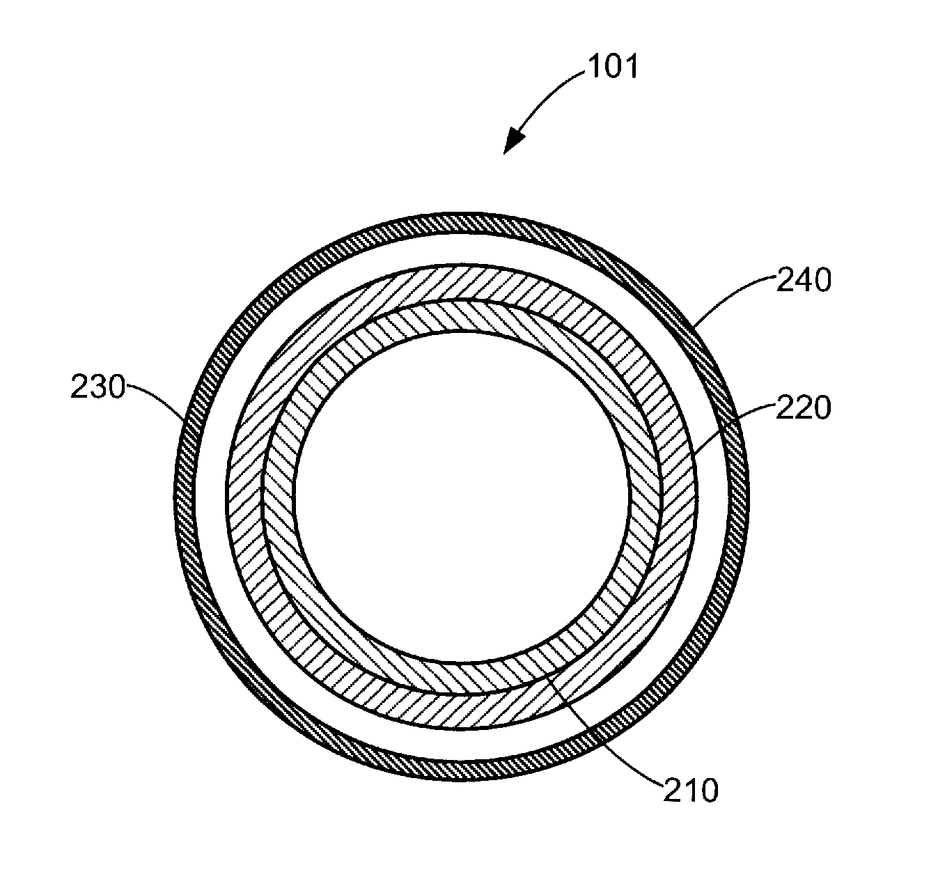
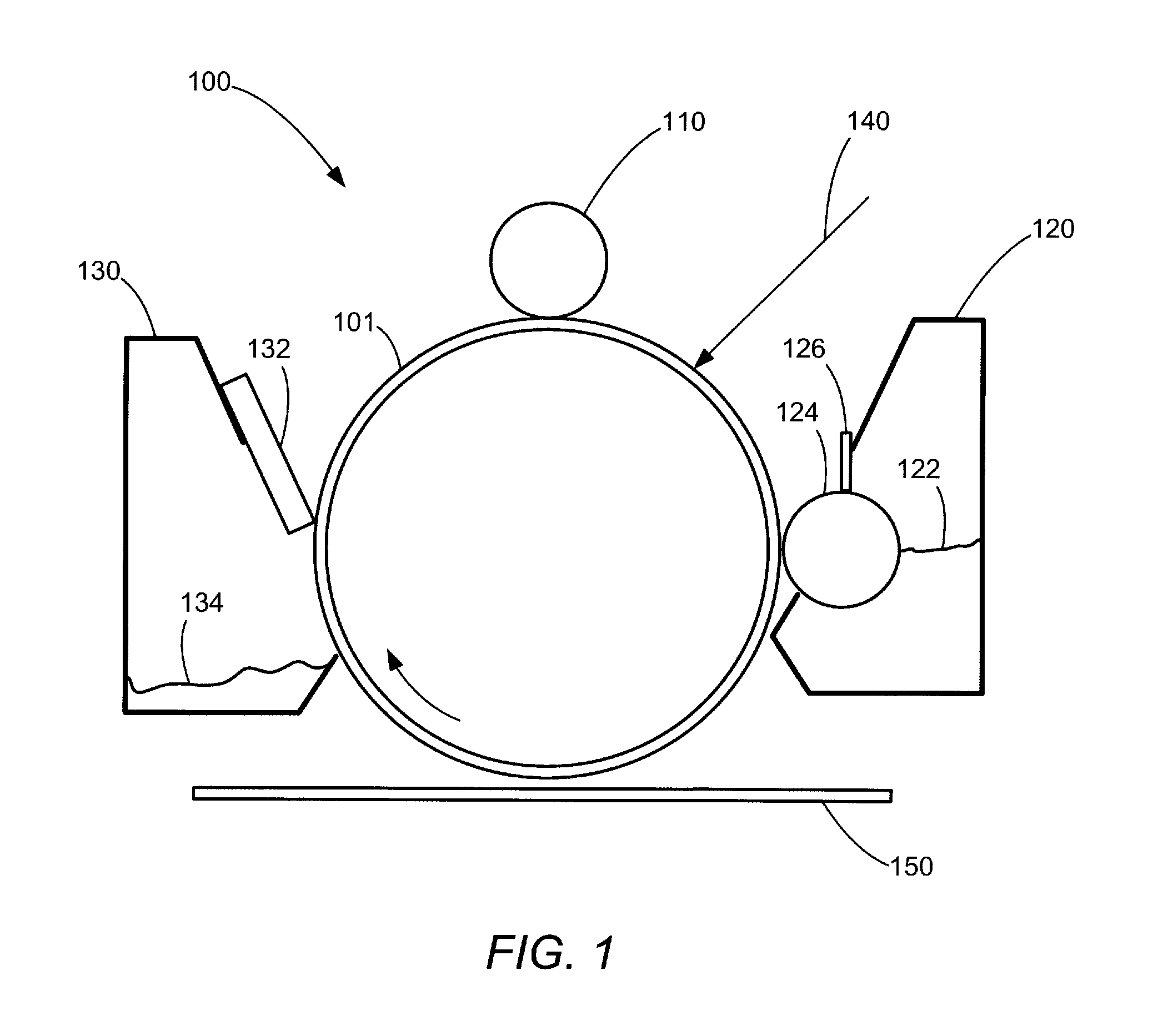
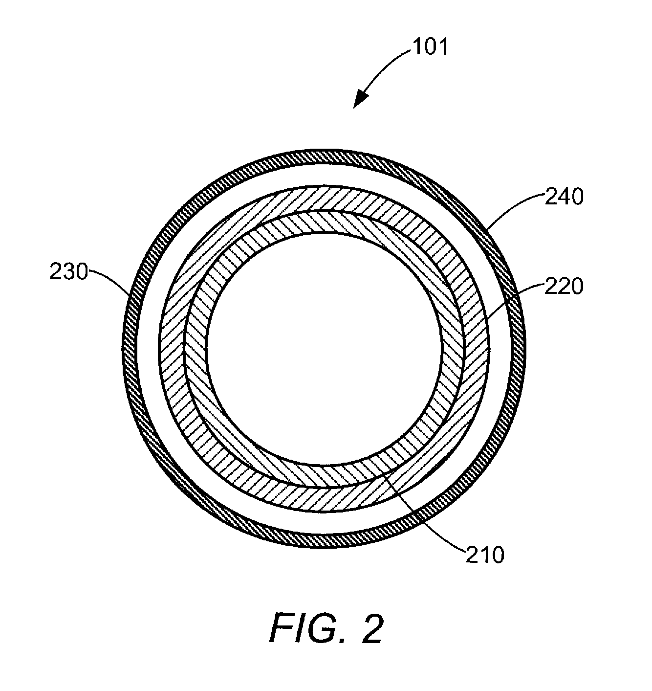
This patent provides an overcoat layer for an organic photoconductor drum in an image forming device. This layer is made from a special UV curable composition that includes a resin with multiple polymerizable groups and a molecule that helps move electric charges. The amount of resin and molecule in the composition are about half of the weight of the final layer. This overcoat layer improves the durability of the photoconductor drum while still allowing electric currents to pass through and generate images. This results in a longer lifespan for the device and a higher number of pages that can be printed before needing replacement.

Problems solved by technology

Conversely, the surface of an organic photoconductor drums is typically comprised of a low molecular weight charge transport material, and an inert polymeric binder and are susceptible to scratches and abrasions.
Therefore, the drawback of using organic photoconductor drums typically arises from mechanical abrasion of the surface layer of the photoconductor drum due to repeated use.
Abrasion of photoconductor drum surface may arise from its interaction with print media (e.g. paper), paper dust, or other components of the electrophotographic image forming device such as the cleaner blade or charge roll.
The abrasion of photoconductor drum surface degrades its electrical properties, such as sensitivity and charging properties.
Electrical degradation results in poor image quality, such as lower optical density, and background fouling.
When a photoconductor drum is locally abraded, images often have black toner bands due to the inability to hold charge in the thinner regions.
This black banding on the print media often marks the end of the life of the photoconductor drum, thereby causing the owner of the printer with no choice but to purchase another expensive photoconductor drum.
However, such overcoat layer does not have the robustness for edge wear of photoconductor drums used in mono (black ink only) printers.
However one major drawback of these overcoats is that they significantly alter the electrophotographic properties of the photoconductor drum in a negative way.
If the overcoat layer is too electrically insulating, the photoconductor drum will not discharge and will result in a poor latent image.
On the other hand, if the overcoat layer is too electrically conducting, then the electrostatic latent image will spread resulting in a blurred image.

Method used


Image

  • Photo conductor overcoat comprising radical polymerizable charge transport molecules and hexa-functional urethane acrylates
  • Photo conductor overcoat comprising radical polymerizable charge transport molecules and hexa-functional urethane acrylates
  • Photo conductor overcoat comprising radical polymerizable charge transport molecules and hexa-functional urethane acrylates

Examples


example 1

[0064]Photoconductor drums were formed using an aluminum substrate, a charge generation layer coated onto the aluminum substrate, and a charge transport layer coated on top of the charge generation layer.

[0065]The charge generation layer was prepared from a dispersion including type IV titanyl phthalocyanine, polyvinylbutyral, poly(methyl-phenyl)siloxane and polyhydroxystyrene at a weight ratio of 45:27.5:24.75:2.75 in a mixture of 2-butanone and cyclohexanone solvents. The polyvinylbutyral is available under the trade name BX-1 by Sekisui Chemical Co., Ltd. The charge generation dispersion was coated onto the aluminum substrate through dip coating and dried at 100° C. for 15 minutes to form the charge generation layer having a thickness of less than 1 μm, specifically a thickness of about 0.2 to about 0.3 μm.

[0066]The charge transport layer was prepared from a formulation including terphenyl diamine derivatives and polycarbonate at a weight ratio of 50:50 in a mixed solvent of THF ...

example 2

[0067]The overcoat layer was prepared from a formulation including 4,4′-di(acrylyloxypropyl)triphenylamine (2 g), EBECRYL 8301 (2 g) and methyl benzoylformate (MBF) photoinitiator (0.2 g) in a mixed solvent of isopropanol and THF. The weight ratio of isopropanol to THF in the mixed solvent was 90:10. The formulation was coated through dip coating on the outer surface of the photoconductor drum formed in Example 1. The coated layer was thermally cured at 60° C. for 5 minutes, then UV cured using Fusion UV H bulb for 5 seconds, and then thermally cured at 120° C. for 60 minutes. The cured layer forms the overcoat layer having a thickness of about 2.8 μm as measured by an eddy current tester. The overcoat thickness may be adjusted by either varying the amount of solvent, or changing the coat speed.

example 3

[0068]The overcoat layer was prepared from a formulation including 4,4′,4″-tri(acryloxypropyl)-triphenylamine (2 g), EBECRYL 8301 (2 g) and MBF photoinitiator (0.2 g) in a mixed solvent of isopropanol and THF. The weight ratio of isopropanol to THF in the mixed solvent was 90:10. The formulation was coated through dip coating on the outer surface of the photoconductor drum formed in Example 1. The coated layer was thermally cured at 60° C. for 10 minutes, then UV cured using Fusion UV H bulb for 5 seconds, and then thermally cured at 120° C. for 60 minutes. The cured layer forms the overcoat layer having a thickness of about 3.3 μm. as measured by an eddy current tester. The overcoat thickness may be adjusted by either varying the amount of solvent, or changing the coat speed.


PUM

PropertyMeasurementUnit
thicknessaaaaaaaaaa
thicknessaaaaaaaaaa
thicknessaaaaaaaaaa

Abstract

An overcoat layer for an organic photoconductor drum of an electrophotographic image forming device is provided. The overcoat layer is prepared from an (UV) ultraviolet curable composition including a urethane resin having at least six radical polymerizable functional groups and a charge transport molecule having at least one radical polymerizable functional group. The amount of the urethane resin having at least six radical polymerizable functional groups in the curable composition is about 35 percent to about 65 percent by weight. The amount of the charge transport molecules having at least one radical polymerizable functional group in the curable composition is about 35 percent to about 65 percent by weight. This overcoat layer improves wear resistance of the organic photoconductor drum without negatively altering the electrophotographic properties, thus protecting the organic photoconductor drum from damage and extending its useful life.

Description

CROSS REFERENCES TO RELATED APPLICATIONS[0001]None.BACKGROUND[0002]1. Field of the Disclosure[0003]The present disclosure relates generally to electrophotographic image forming devices, and more particularly to an overcoat layer for an organic photoconductor drum having excellent abrasion resistance and electrical properties.[0004]2. Description of the Related Art[0005]Organic photoconductor drums have generally replaced inorganic photoconductor drums in electrophotographic image forming device including copiers, facsimiles and laser printers due to their superior performance and numerous advantages compared to inorganic photoconductors. These advantages include improved optical properties such as having a wide range of light absorbing wavelengths, improved electrical properties such as having high sensitivity and stable chargeability, availability of materials, good manufacturability, low cost, and low toxicity.[0006]While the above enumerated performance and advantages exhibited b...

Claims


Application Information

Patent Timeline
Patent Type & Authority Patents(United States)
IPC IPC(8): G03G5/00G03G5/147
CPCG03G5/14769G03G5/14786G03G5/14791G03G5/14734G03G5/0618
Inventor BELLINO, MARK THOMASBLACK, DAVID GLENLUO, WEIMEIREEVES, SCOTT DANIEL
Owner LEXMARK INT INC
Learn More