Methods of selectively forming a material using parylene coating

Active Publication Date: 2015-02-03
MICRON TECH INC
View PDF10 Cites 311 Cited by
  • Summary
  • Abstract
  • Description
  • Claims
  • Application Information

AI Technical Summary

Problems solved by technology

However, the ability to pattern organic materials using conventional lithographic techniques is limited since it is only possible to alter functional groups or deposit materials on horizontal surfaces of the substrate, not on surfaces of recessed structures in the substrate.
Furthermore, conventional blocking m

Method used


Image

  • Methods of selectively forming a material using parylene coating
  • Methods of selectively forming a material using parylene coating
  • Methods of selectively forming a material using parylene coating

Examples


Embodiment Construction

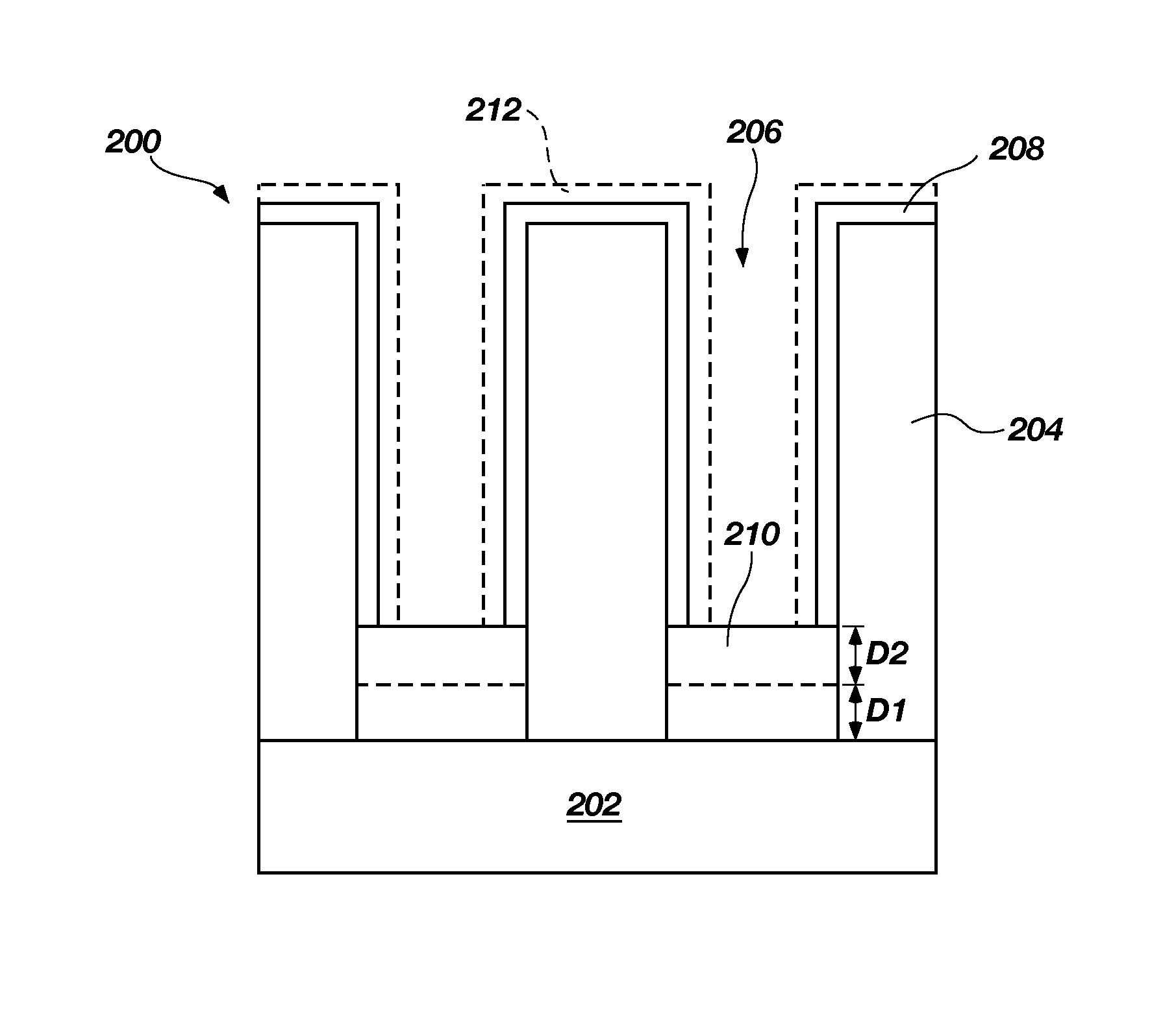
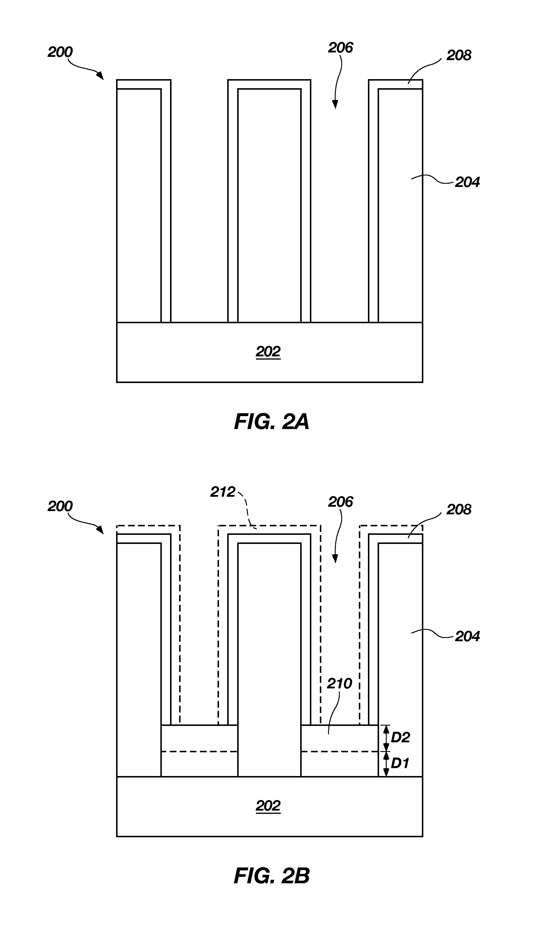
[0010]The illustrations presented herein are not meant to be actual views of any particular component, device, or system, but are merely idealized representations that are employed to describe embodiments of the present invention.

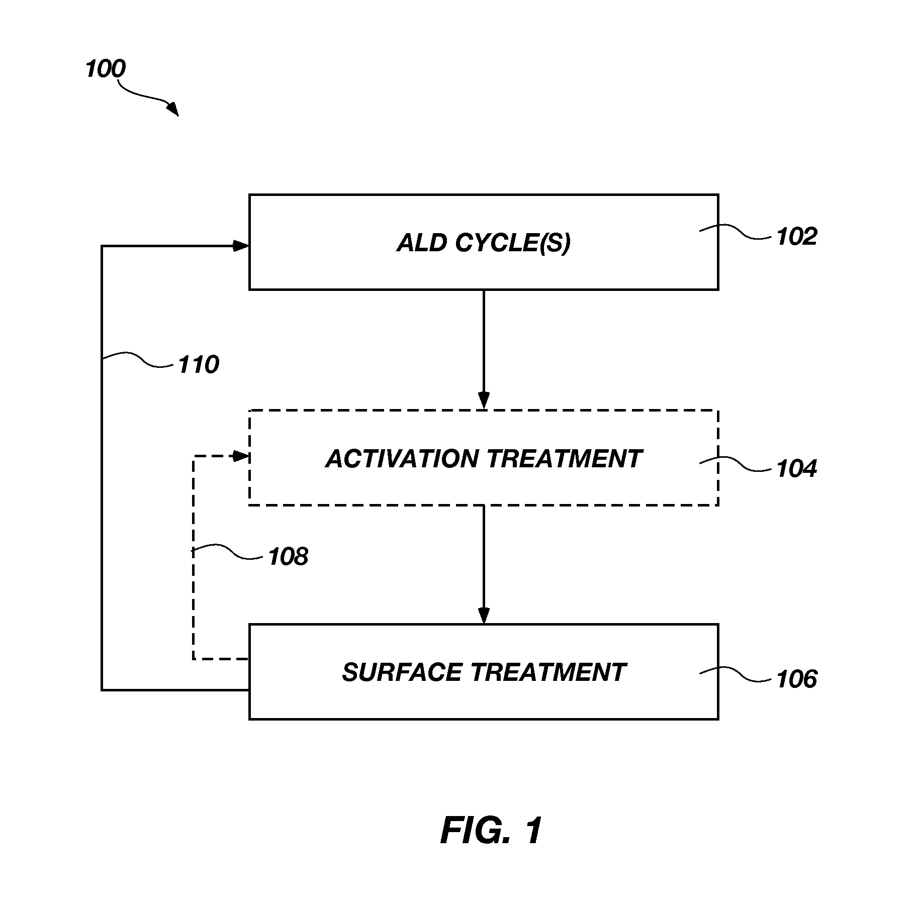
[0011]As used herein, the terms “atomic layer deposition” and “ALD” mean and include a deposition process in which a plurality of consecutive deposition cycles is conducted in a reaction chamber or a deposition chamber.

[0012]As used herein, the term “ALD process” means and includes a process of forming a material using ALD and the term “ALD material” means and includes a material formed by an ALD process.

[0013]As used herein, the term “ALD cycle” means and includes sequentially introducing each precursor into a reaction chamber or a deposition chamber separately followed by pumping / purging the reaction chamber or the deposition chamber with an inert gas to prevent mixing or reacting of the precursors.

[0014]As used herein, the term “substrate” means and incl...


PUM

PropertyMeasurementUnit
Thicknessaaaaaaaaaa

Abstract

Methods for depositing a material, such as a metal or a transition metal oxide, using an ALD (atomic layer deposition) process and resulting structures are disclosed. Such methods include treating a surface of a semiconductor structure periodically throughout the ALD process to regenerate a blocking material or to coat a blocking material that enables selective deposition of the material on a surface of a substrate. The surface treatment may reactivate a surface of the substrate toward the blocking material, may restore the blocking material after degradation occurs during the ALD process, and/or may coat the blocking material to prevent further degradation during the ALD process. For example, the surface treatment may be applied after performing one or more ALD cycles. Accordingly, the presently disclosed methods enable in situ restoration of blocking materials in ALD process that are generally incompatible with the blocking material and also enables selective deposition in recessed structures.

Description

TECHNICAL FIELD[0001]The invention, in various embodiments, relates generally to methods for performing atomic layer deposition (ALD). More particularly, this disclosure relates to methods of performing area-selective ALD.BACKGROUND[0002]ALD processes are used to produce thin, conformal films having high thickness accuracy and step coverage. ALD utilizes a series of sequential, self-limiting surface reactions, each forming a monolayer of adsorbed precursor, to form the film. ALD provides atomic layer control and enables the films to be deposited on structures having high aspect ratios. ALD conventionally uses two or more gaseous precursors, each being sequentially introduced into a reaction chamber. A wide variety of materials may be deposited by ALD, many of which are used in the fabrication of semiconductor devices and integrated circuits (ICs).[0003]In a conventional ALD process, at least one precursor is introduced to a substrate in a reaction chamber in alternate pulses separat...

Claims


Application Information

Patent Timeline
IPC IPC(8): C30B25/04C23C16/02C23C16/04C23C16/455H01L21/02H01L21/285H01L21/768
CPCH01L21/0228C23C16/0227C23C16/042C23C16/045C23C16/45534H01L21/02175H01L21/02304H01L21/28562H01L21/76879H01L21/02118H01L21/02181H01L21/02186H01L21/02192H01L21/02194H01L21/32051
Inventor MARSH, EUGENE P.
Owner MICRON TECH INC
Why Eureka
Try Eureka