

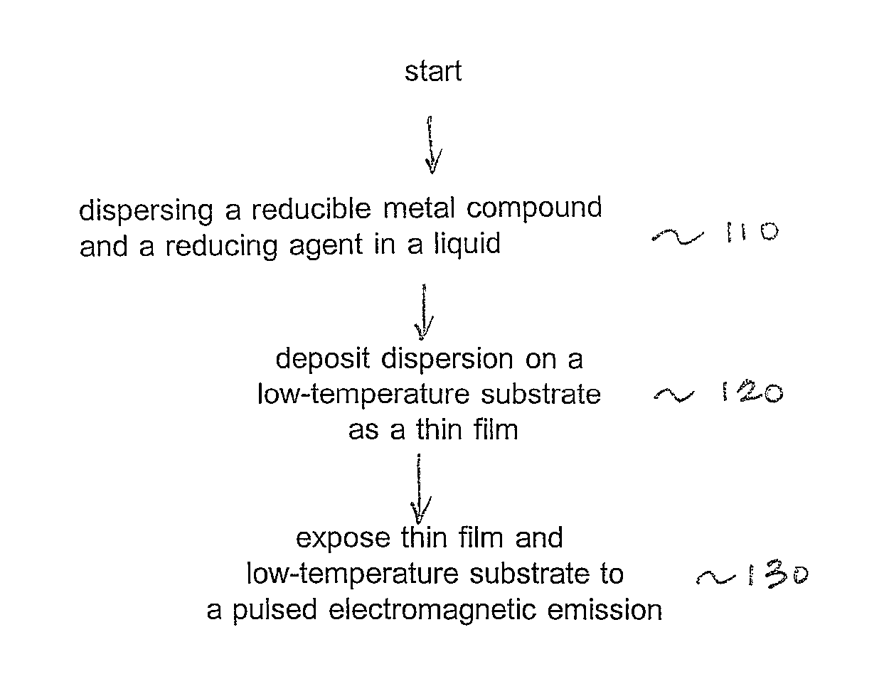
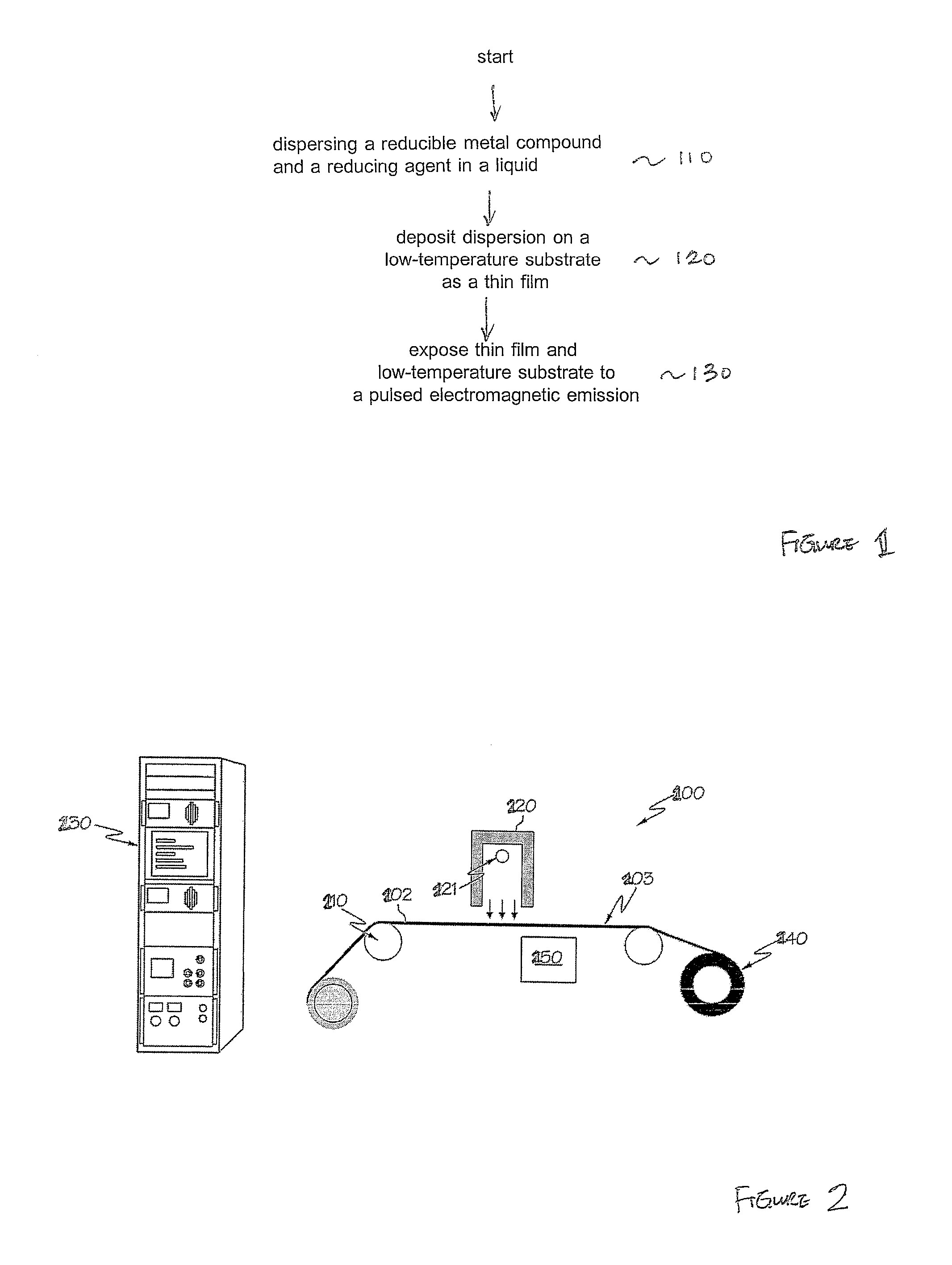
Method for reducing thin films on low temperature substrates
a technology of low temperature substrates and thin films, applied in the field of cure methods, can solve the problems of preventing the use of inexpensive substrates, high cost of conductive traces, and limited sintering
- Summary
- Abstract
- Description
- Claims
- Application Information
AI Technical Summary
Problems solved by technology
Method used
Image

Examples
example 1
Ascorbic Acid Reducer
[0040]A copper oxide dispersion was produced by mixing 3.0 g<50 nm copper (II) oxide, 3.6 g deionized water, 0.15 g PVP K-30, 0.3 g ethylene glycol, 0.04 g Tergitol® TMN-6, 0.02 g Dynol® 604, 0.02 g BYK®-020, and 0.66 g ascorbic acid in a 20 mL vial. 5 g of zirconium oxide milling media was added and the vial was agitated for 60 minutes.
[0041]The dispersion was applied to a sheet of Melinex® ST505 PET by drawdown using a #5 Meyer bar.
[0042]The sample was cured with a pulse length of 1,000 microseconds, and overlap factor of 2 at 24 feet per minute in an air environment. Although the film was not electrically conductive, the color of the film changed from dark brown to a copper color indicating significant conversion of the copper oxide to copper.
example 2
Ethylene Glycol / Glycerol Reducer
[0043]A copper oxide dispersion was produced by mixing 2.0 g NanoArc® copper oxide, 5.7 g deionized water, 0.10 g PVP K-30, 0.6 g ethylene glycol, 0.03 g Tergitol® TMN-6, 0.01 g Dynol® 604, and 0.32 g glycerol in a 20 mL vial. 5 g of zirconium oxide milling media was added and the vial was agitated for 60 minutes.
[0044]The dispersion was applied to a sheet of Melinex® ST505 PET by drawdown using a #5 Meyer bar.
[0045]The sample was cured with a pulse length of 850 microseconds, and overlap factor of 2 at 24 feet per minute in an air environment. Although the film was not electrically conductive, the color of the film changed from dark brown to a copper color indicating significant conversion of the copper oxide to copper.
example 3
Ethylene Glycol / Glycerol Reducer
[0046]A copper oxide dispersion was produced by mixing 2.0 g NanoArc® copper oxide, 5.4 g deionized water, 0.10 g PVP K-30, 0.6 g ethylene glycol, 0.03 g Tergitol® TMN-6, 0.01 g Dynol® 604, and 0.67 g glycerol in a 20 mL vial. 5 g of zirconium oxide milling media was added and the vial was agitated for 60 minutes.
[0047]The dispersion was applied to a sheet of Melinex® ST505 PET by drawdown using a #5 Meyer bar.
[0048]The sample was cured with a pulse length of 1,000 microseconds, and overlap factor of 3 at 24 feet per minute in an air environment. Although the film was not electrically conductive, the color of the film changed from dark brown to a copper color indicating significant conversion of the copper oxide to copper.
PUM
| Property | Measurement | Unit |
|---|---|---|
| temperature | aaaaa | aaaaa |
| melting point | aaaaa | aaaaa |
| thick | aaaaa | aaaaa |
Abstract
Description
Claims
Application Information