Conformal electromagnetic (EM) detector

a detector and electromagnetic technology, applied in the direction of electrical apparatus construction details, semiconductor/solid-state device details, electrical apparatus contruction details, etc., can solve the problems of heavy and bulky detection solutions, and achieve the effect of easy removal and easy application

Inactive Publication Date: 2015-02-03
LOCKHEED MARTIN CORP
View PDF57 Cites 86 Cited by
  • Summary
  • Abstract
  • Description
  • Claims
  • Application Information

AI Technical Summary

Benefits of technology

[0007]In view of the foregoing, it would be an advance in the art to create inexpensive, conformal, organic-based detectors that can be replaced / maintained / updated independently of the associated read-out electronics. It would also be an advance in the art to create a conformal EM and / or x-ray detection coating that can be easily applied to a wide range of surfaces of varying shape and contour. It would also be an advance in the art to create a conformal EM detection coating that can be easily removed to allow for maintenance of the underlying components and / or substrates.
[0010]Variations of a deposition process for an insulating / protective layer may include spraying, dispensing, powder-coating, laminating, painting, vapor deposition, flame spray, or submerging the component(s) in a desired insulating / protective material such as elastomer, silicone, latex, ceramic, glass, or other suitable material which may allow for easy removal of the coating. Variations of a protective layer may include directly written silicone or sprayed-on urethane. Further variations of a protective layer may include acrylic, parylene, kraton, noryl, etc. In some cases, a urethane layer may provide improved adhesion between the protective layer and the coated surface.

Problems solved by technology

Such detection solutions tend to be heavy and bulky.
They also are usually flat, requiring that the subject of an x-ray be positioned in potentially uncomfortable and / or otherwise cumbersome positions to properly image a particular component portion or body part.

Method used


Image

  • Conformal electromagnetic (EM) detector
  • Conformal electromagnetic (EM) detector
  • Conformal electromagnetic (EM) detector

Examples


Embodiment Construction

[0029]The following detailed description of the invention refers to the accompanying drawings. The same reference numbers in different drawings identify the same or similar elements. Also, the following detailed description does not limit the invention. Instead, the scope of the invention is defined by the appended claims and equivalents thereof.

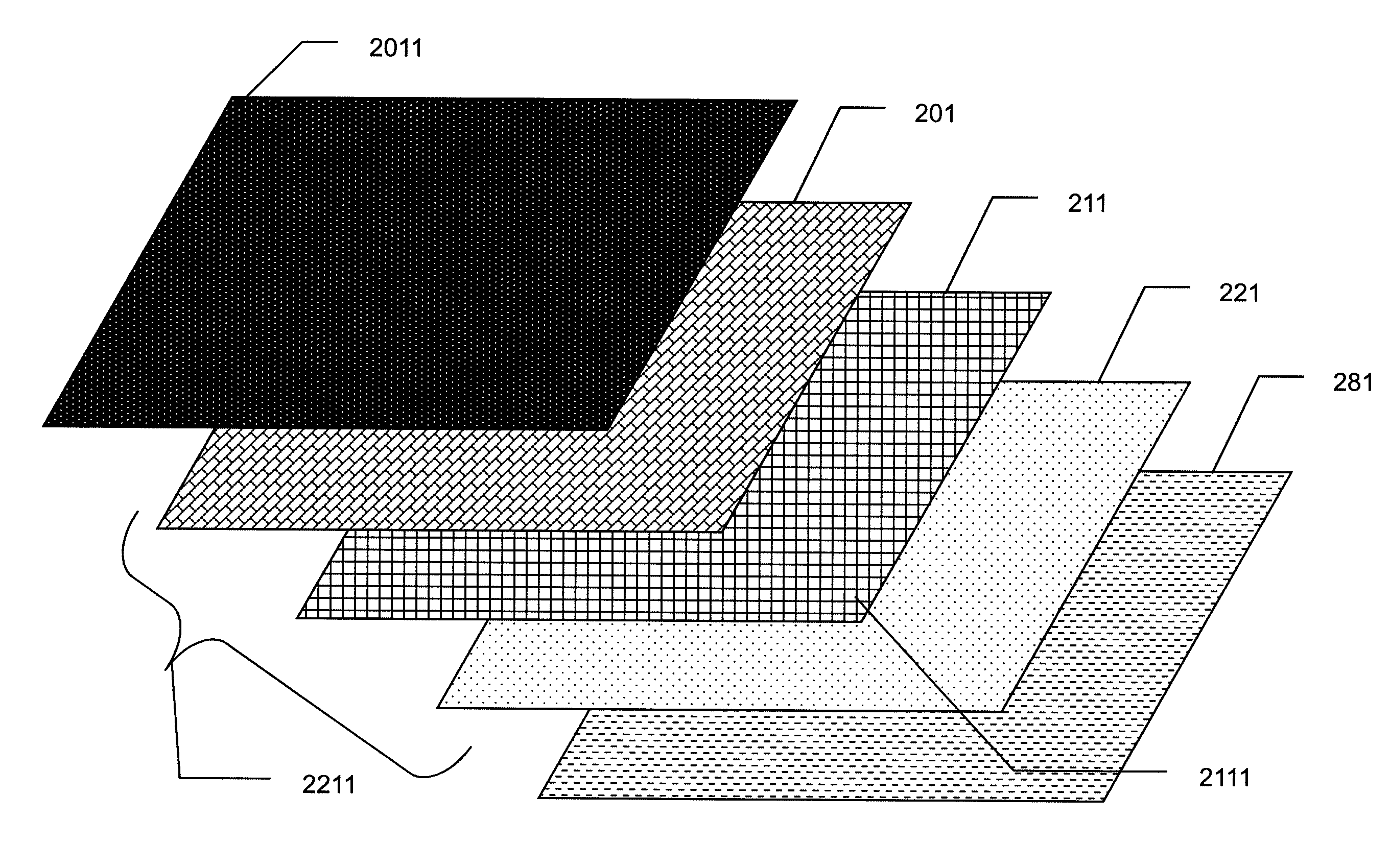
[0030]In one variation, a conformal electro-magnetic detector may include at an electrically insulating layer disposed onto the substrate and / or component surface and an electrically conductive layer that connects electrically to logic or monitoring circuitry disposed on top of the insulating layer.

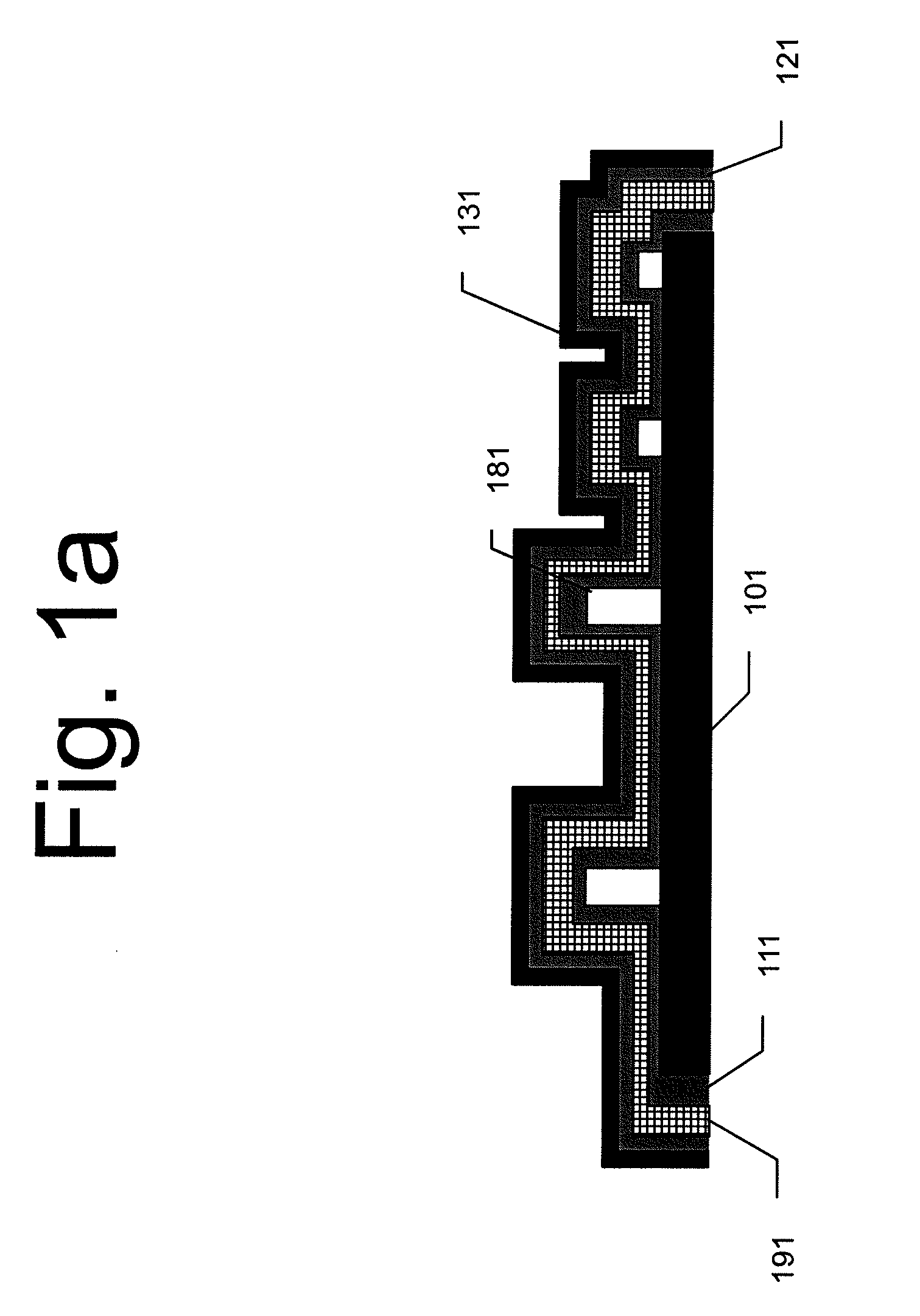
[0031]A variation of the type discussed above is depicted in FIG. 1a. In the variation shown, a component board 101 having electronic, electro-optical and / or electro-mechanical components 181 mounted thereon is covered with a conformal insulating layer 111 that minimally alters the shape and footprint of the board (if at all). In some variations, ...


PUM


Abstract

A conformal electro-magnetic (EM) detector and a method of applying such a detector are provided herein as well as variations thereof Variations include, but are not limited to, single-element, area detectors; an array of multiple active elements.

Description

PRIORITY[0001]The present application is a continuation in-part of U.S. patent application Ser. No. 12 / 904,854, filed in the U.S. Patent and Trademark Office on Oct. 14, 2010, the entire contents of which are hereby incorporated by reference.FIELD OF THE INVENTION[0002]The present invention relates generally to electromagnetic and electro-optical detection solutions to protect components or information stored in electronic or optical modules, components of a printed circuit or wiring board, or in integrated circuits or optical devices.BACKGROUND OF THE INVENTION[0003]Organic devices are quickly replacing standard silicon-based devices due to the ability to use inexpensive roll-to-roll processing for higher throughput. Organic light emitting diodes (OLEDs) and organic photovoltaic (PV) cells are two such examples. OLEDs are now commonplace in small displays and in cell phones because of the advantages over LCD screens (e.g. no backlighting required, photonic materials are printed ine...

Claims


Application Information

Patent Timeline
Patent Type & Authority Patents(United States)
IPC IPC(8): H05K7/14H05K9/00H05K7/18H01L23/00H01L27/30H05K1/02H05K3/28
CPCH01L23/573H01L27/305H01L27/308H05K1/0275H01L2924/09701H01L2924/12044H01L2924/3011H05K3/284H05K2201/09872H01L2924/0002H01L2924/00H10K39/36H10K39/30
Inventor KELLEY, MATTHEWADAMS, CHRISTIANREIM, RICHARD
Owner LOCKHEED MARTIN CORP
Why Eureka
Try Eureka