Clock generator and method thereof

a clock generator and clock technology, applied in the field of electronic devices, can solve the problems of sampling timing mismatch between the n analog-to-digital converters, non-ideal problems of time-interleaved analog-to-digital converters, timing skew, etc., and achieve the effect of reducing the mismatch problem

Active Publication Date: 2015-02-24
REALTEK SEMICON CORP
View PDF2 Cites 1 Cited by
  • Summary
  • Abstract
  • Description
  • Claims
  • Application Information

AI Technical Summary

Benefits of technology

[0009]One object of the invention is to provide a clock generation device and a method thereof to prevent from the mismatch problem of multiple clock paths in a conventional clock generation device.
[0010]One object of the invention is to provide a clock generation device and a method thereof to prevent from the time mismatch problem of multiple clocks in a conventional clock generation device.
[0014]The clock generation device and the clock generation method according to the present invention uses logic circuits to control the stop-sampling edges of the output clocks without the mismatch problem due to misalignment of sampling timing. Besides, no longer delay path like the prior art is required so as to reduce the mismatch problem caused by mismatch of the path lengths between the output clocks generated by the clock generation device of the prior art. Non-overlapping clocks can be provided precisely and the mismatch problem due to long signal paths in the prior art can be resolved.

Problems solved by technology

In an N-channel time-interleaved analog-to-digital converter, “N” (N is a positive integer) analog-to-digital converters are connected in parallel to form N channels to increase the sampling rate of the analog-to-digital converter by N times. However, a time-interleaved analog-to-digital converter still has non-ideal problems, such as sampling timing mismatch between the N analog-to-digital converters (i.e., sampling timing skew) or gain mismatch and offset mismatch between the N analog-to-digital converters.
Sampling timing mismatch is due to different sampling cycles of the channels of analog-to-digital converters.
Practically, the sampling timing between channels of the analog-to-digital converters cannot be set to a 1-ns interval accurately, resulting in sampling timing mismatch of N analog-to-digital converters.
Sampling timing mismatch is caused by different signal path lengths of the signal sources of the analog-to-digital converters and an asymmetric circuit configuration.
Since the path from the clock CLKin to the clock CK1 and the path from the clock CLKin to the clock CK2 cannot be too short and there are physical limitations in chip fabrication to fabricate exactly the same elements, the mismatch between the path from the clock CLKin to the clock CK1 and the path from the clock CLKin to the clock CK2 causes the 2-channel time-interleaved analog-to-digital converter to have sampling timing mismatch to reduce circuitry performance.

Method used


Image

  • Clock generator and method thereof
  • Clock generator and method thereof
  • Clock generator and method thereof

Examples


Embodiment Construction

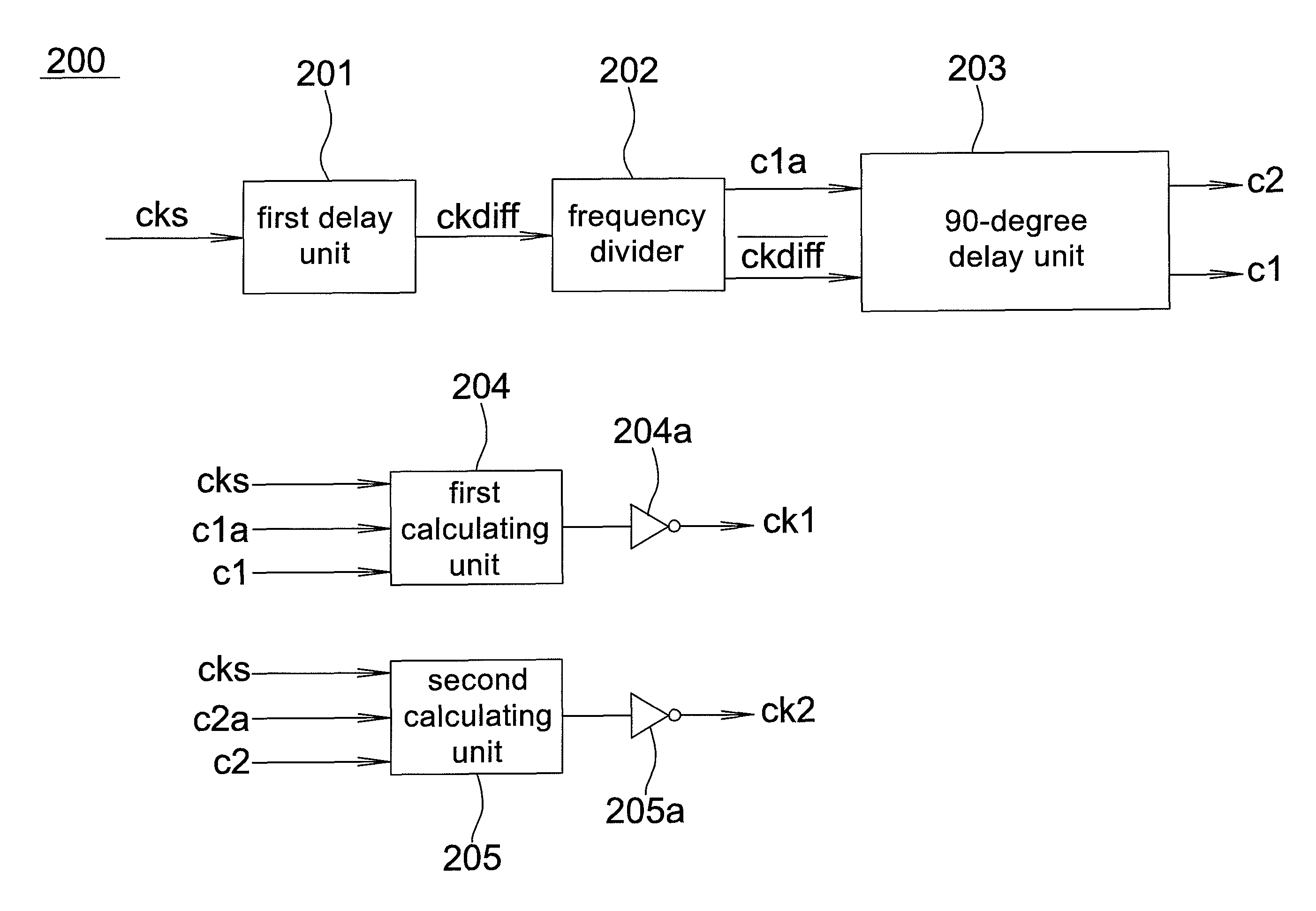
[0025]FIG. 2A shows a schematic diagram illustrating a clock generation device in an embodiment of the invention. The clock generation device 200 is a divide-by-N clock generator having low sampling timing skew. The clock generation device 200 comprises a first delay unit 201, a frequency divider 202, a 90-degree delay unit 203, a first calculating unit 204, and a second calculating unit 205.

[0026]The first delay unit 201 receives an input clock cks and delays the input clock cks by a preset period dl to generate an input delay clock ckdiff.

[0027]The frequency divider 202 receives the input delay clock ckdiff, outputs an inverted input delay clock ckdiff and divides the frequency of the input delay clock ckdiff to generate a first frequency-divided clock c1a and a second frequency-divided clock c2a (not shown in the figure). The frequency of each of the first frequency-divided clock c1a and the second frequency-divided clock c2a is a preset multiple (1 / N where N is a nature number l...


PUM


Abstract

A clock generation device includes a first delay unit, a frequency divider, an angle delay unit and a first calculating unit. The first delay unit receives an input clock and delays the input clock by a first preset period to generate an input delay clock. The frequency divider divides a frequency of the delay clock to generate a first frequency-divided clock and a second frequency-divided clock. A frequency of each of the first frequency-divided clock and the second frequency-divided clock is a preset multiple of the input delay clock. The angle delay unit delays the first frequency-divided clock by a second preset period to generate a first delay clock. The first calculating unit determines a trigger time of a first edge of a first output clock with reference to voltage levels of the first frequency-divided clock and the first delay clock and determines a falling time of a second edge of the first output clock with reference to voltage levels of the input clock and the first delay clock.

Description

[0001]This application claims the benefit of the filing date of Taiwan Application Ser. No. TW 102112446, filed on Apr. 9, 2013, the content of which is incorporated herein by reference.BACKGROUND OF THE INVENTION[0002](a) Field of the Invention[0003]The invention relates to an electronic device, particularly to a clock generation device and method thereof.[0004](b) Description of the Related Art[0005]In an N-channel time-interleaved analog-to-digital converter, “N” (N is a positive integer) analog-to-digital converters are connected in parallel to form N channels to increase the sampling rate of the analog-to-digital converter by N times. However, a time-interleaved analog-to-digital converter still has non-ideal problems, such as sampling timing mismatch between the N analog-to-digital converters (i.e., sampling timing skew) or gain mismatch and offset mismatch between the N analog-to-digital converters.[0006]Sampling timing mismatch is due to different sampling cycles of the chan...

Claims


Application Information

Patent Timeline
Patent Type & Authority Patents(United States)
IPC IPC(8): G06F1/04H03K3/86
CPCH03K3/86H03K5/15013
Inventor HUANG, SHIH-HSIUNLIN, SHIAN-RU
Owner REALTEK SEMICON CORP
Why Eureka
Try Eureka