Supercharge Your Innovation With Domain-Expert AI Agents!

Memory interface chip corresponding to different memories and method of establishing memory transmission channel

a technology of memory interface and memory transmission channel, which is applied in the direction of electric digital data processing, instruments, etc., can solve the problems of limited output bandwidth and overall data transmission rate of thick-oxide units, inability to significantly reduce the data transmission interface of data processing modules, and not being suitable for processing different interface voltages

Active Publication Date: 2015-03-03
XUESHAN TECH INC
View PDF6 Cites 0 Cited by
  • Summary
  • Abstract
  • Description
  • Claims
  • Application Information

AI Technical Summary

Benefits of technology

This patent describes a memory interface chip that can work with different types of memory structures and operate at different data transmission bandwidths and interface voltages. The chip includes a data output unit and a control module that can selectively connect to different memories. The control module can choose the most appropriate output or receiving channel for the memory based on its structure and interface voltage. This allows the chip to have flexibility and adapt to different needs. Its technical effects are improved performance and reliability for different memory systems.

Problems solved by technology

However, the dimension of the data transmission interface of the data processing module can't be significantly reduced due to the use of many analogue front ends.
However, the analogue front ends of DDR2 SDRAMs for processing different interface voltages use different components and therefore are not suitable for processing different interface voltages.
When the analogue front ends using thick-oxide units are used to process low interface voltages, the output bandwidth and overall data transmission rate of the thick-oxide units will be limited.
On the other hand, when the analogue front ends made of thin-oxide units are used to process normal interface voltages, the higher interface voltages will damage the thin-oxide units of the analogue front ends and cause malfunction.
Thus, it can be seen that using memories with different bandwidths and interface voltages while maintaining the overall data transmission rate of the analogue front end is indeed an important issue in the data transmission technology.

Method used


Image

  • Memory interface chip corresponding to different memories and method of establishing memory transmission channel
  • Memory interface chip corresponding to different memories and method of establishing memory transmission channel
  • Memory interface chip corresponding to different memories and method of establishing memory transmission channel

Examples


Embodiment Construction

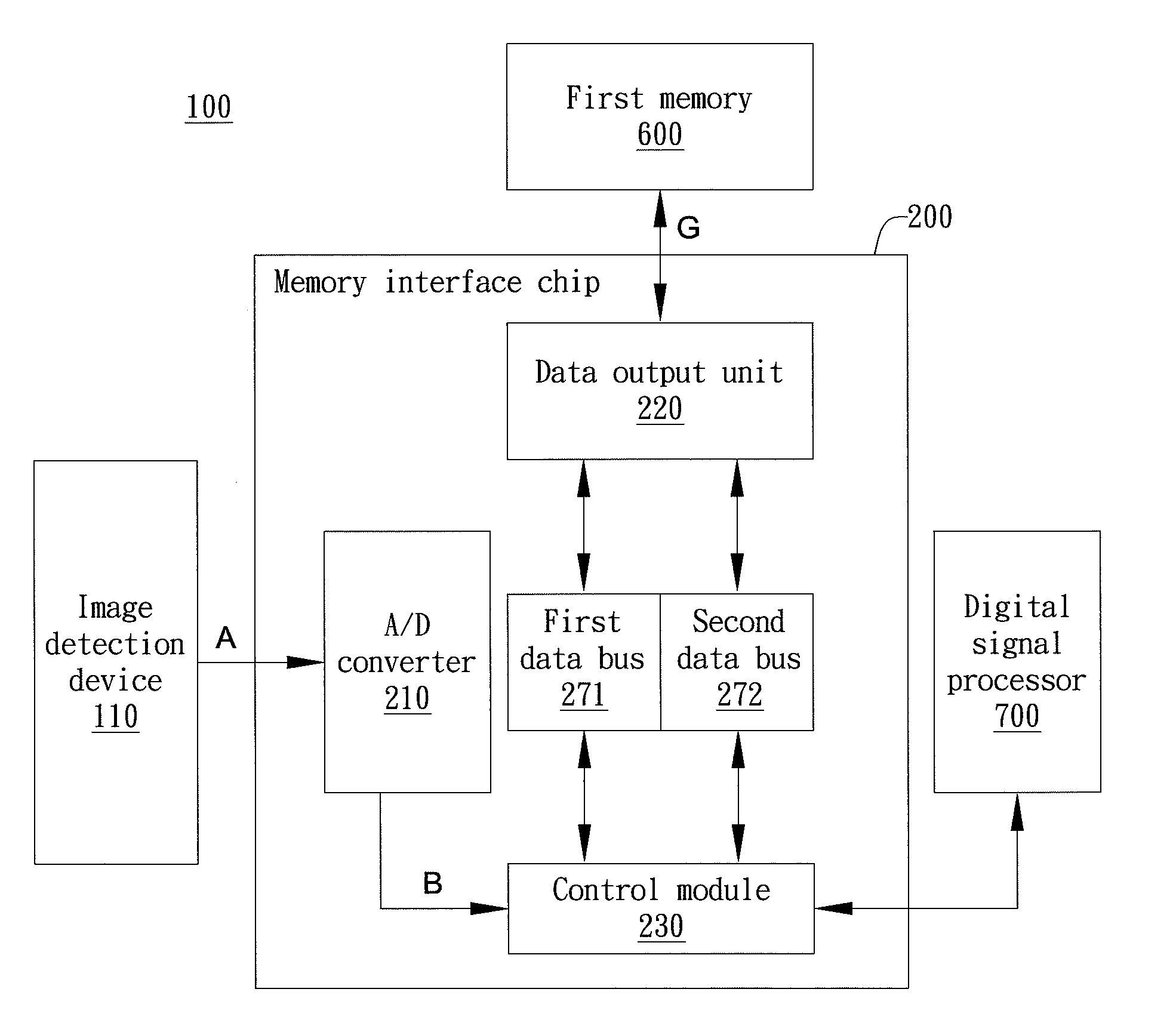
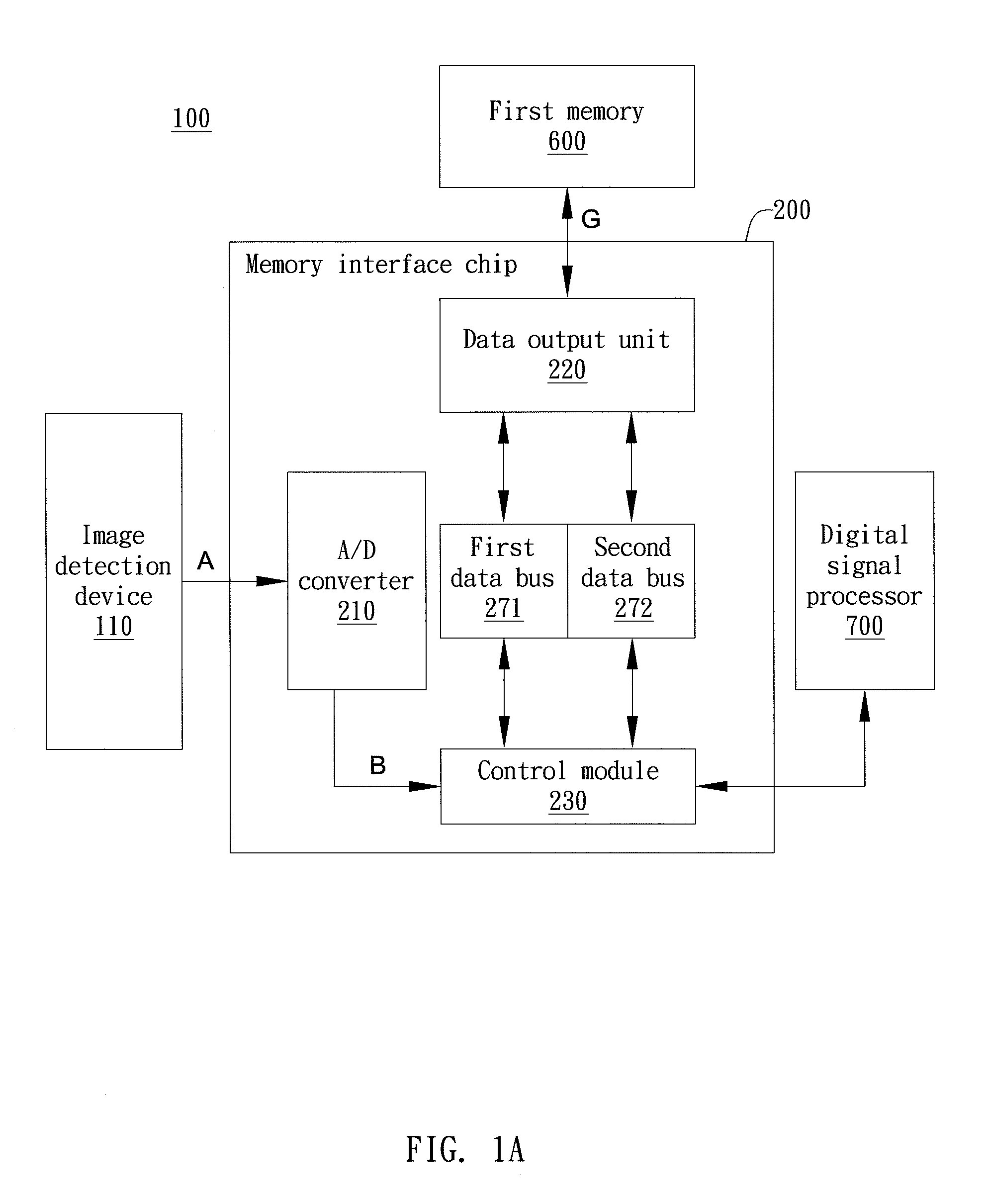
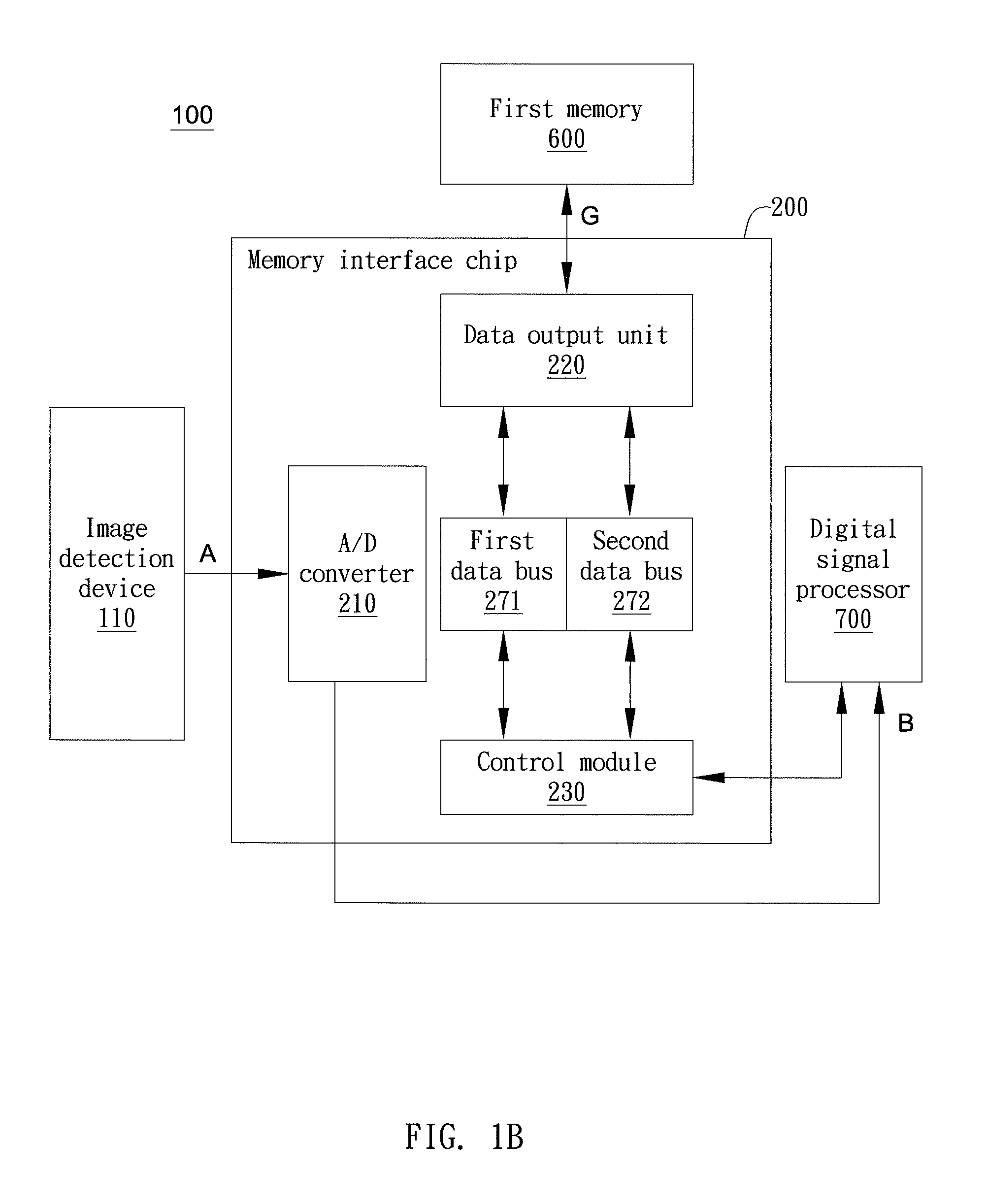
[0023]The present invention relates to a memory interface chip and preferably a memory interface chip for processing image data and corresponding to different memory structures. The memory interface chip is connected to a digital signal source to receive and process the digital data signal and then transmit the processed digital data signal to a data processing system such as digital cameras or personal computers. The memory interface chip includes a plurality of output channels corresponding to different memory structures and memories using different interface voltages such as Double Data Rate Synchronous Dynamic Random Access Memory (DDR SDRAM) and Double Data Rate Two Synchronous Dynamic Random Access Memory (DDR2 SDRAM). The memory interface chip can selectively close off at least one of the output channels based on the structure or interface voltage of the memory used.

[0024]FIG. 1A is a block diagram of an image processing device 100. As FIG. 1A shows, the image processing devi...


PUM


Abstract

A memory interface chip is disclosed and includes a data output unit and a control module, wherein the data output module receives data from an external source. The data output unit can be selectively connected to different memory structures. The data output unit includes a first output channel and a second output channel, wherein the channels respectively generate a first output signal and a second output signal based on the data received. The control module selectively closes off the first output channel or the second output channel based on the memory architecture of the memory connected to the data output unit.

Description

1. FIELD OF THE INVENTION[0001]This invention relates to a memory interface chip; specifically a memory interface chip for processing image data and corresponding to different memories structures.2. DESCRIPTION OF THE PRIOR ART[0002]In the field of data processing technology, the data processing module for processing electrical signals may use different memory structures for different purposes. For instance, while encoding / decoding image signals, the data processing module normally uses the Double-Data-Rate Two Synchronous Dynamic Random Access Memory (DDR2 SDRAM) to process image signals. On the other hand, while processing audio signals, the data processing module normally use Double-Data-Rate Synchronous Dynamic Random Access Memory (DDR SDRAM) to process audio signals.[0003]Different memory structures and specifications have different data bus interface and interface voltages. Therefore, the data processing module using different types of memories normally includes a data transm...

Claims


Application Information

Patent Timeline
Patent Type & Authority Patents(United States)
IPC IPC(8): G06F13/12
CPCG06F13/12G06F13/1684
Inventor LIN, CHUN-FUSUN, CHIH-KUO
Owner XUESHAN TECH INC
Features
  • R&D
  • Intellectual Property
  • Life Sciences
  • Materials
  • Tech Scout
  • Unparalleled Data Quality
  • Higher Quality Content
  • 60% Fewer Hallucinations
Learn More