Semiconductor integrated circuit and optical sensor device using the same

a technology of semiconductor integrated circuit and optical sensor, which is applied in the direction of photometry using electric radiation detectors, pulse techniques, instruments, etc., can solve the problems of reducing affecting so as to reduce the number of fuses to be melted and cut, the effect of preventing adverse effects on the quality of semiconductor integrated circuit, and suppressing adverse effects on the quality of semiconductor

Active Publication Date: 2015-04-07
SHARP KK
View PDF10 Cites 4 Cited by
  • Summary
  • Abstract
  • Description
  • Claims
  • Application Information

AI Technical Summary

Benefits of technology

[0070]As apparent from the above description, in the semiconductor integrated circuit of this invention, as trimming information for a case where a characteristic value of the operation circuit is a mean value in the appearance frequency distribution of the characteristic value, trimming information representing that the number of melted-and-cut fuses in the trimming information generation circuit is the least possible number is assigned, and as the trimming information for cases where the characteristic value falls within the range of {the mean value±2×(standard deviation)} in the appearance frequency distribution, trimming information representing that the number of melted-and-cut fuses is a second least number next to the least number is assigned.
[0071]Further, by the conversion circuit, a bit string of the trimming information outputted from the trimming information generation circuit is converted into the element selection information representing whether or not each of the plurality of elements in the element array is turned off by a bit string associated with the individual elements.
[0072]Thus, the number of melted-and-cut fuses involved in trimming on manufactured products in which the characteristic value before correction falls within the range of {the mean value±2×(standard deviation)} in the appearance frequency distribution of the characteristic value can be lessened. As a result, damage to the semiconductor due to melt-and-cut of the fuses in trimming process can be lessened, so that adverse effects on the quality of the semiconductor integrated circuit can be suppressed.
[0073]In particular, as the trimming information for the case where the characteristic value before correction from the operation circuit is a mean value in the appearance frequency distribution, trimming information representing that the number of melted-and-cut fuses is the least number is assigned. Therefore, in trimming for most manufactured products in which “the characteristic value before correction is a mean value in the appearance frequency distribution,” the number of melted-and-cut fuses can be made to be the least one, so that adverse effects on the quality of the semiconductor integrated circuit can be prevented.
[0074]Also, according to the optical sensor device of this invention, the semiconductor integrated circuit of the invention is mounted on at least either one of the light-emission control circuit and the light-receiving circuit, the semiconductor integrated circuit being capable of lessening the number of melted-and-cut fuses for manufactured products in which the characteristic value before correction falls within the range of {the mean value±2×(standard deviation)} in the characteristic-value appearance frequency distribution, and reducing damage to the semiconductor due to melt-and-cut of the fuses, so that adverse effects on the quality can be suppressed. Therefore, variations in light-reception sensitivity characteristic and variations in light-emission intensity characteristic can be suppressed without impairing the quality of the light-emission control circuit and the light-receiving circuit.
[0075]Thus, occurrence of defective products can be suppressed, allowing a cost reduction to be achieved.

Problems solved by technology

In manufacture of such optical sensors, variations in light-reception sensitivity or characteristic variations in light-emission intensity have been at issue.
In this case, since the melt-and-cut of the fuses causes the semiconductor integrated circuit to be damaged, the number of fuses to be melted and cut is desirably as small as possible.
However, the prior-art semiconductor integrated circuit device 5 shown above has problems as shown below.
That is, the melt-and-cut of fuses causes the semiconductor to be damaged to a considerable extent.
Also, there is a fear for occurrence of a problem in reliability of the melt-and-cut, giving adverse effects on the quality.

Method used


Image

  • Semiconductor integrated circuit and optical sensor device using the same
  • Semiconductor integrated circuit and optical sensor device using the same
  • Semiconductor integrated circuit and optical sensor device using the same

Examples


first embodiment

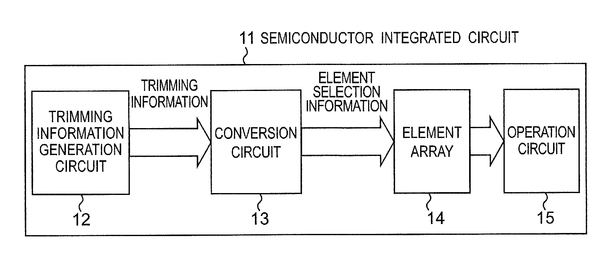
[0090]FIG. 1 is an outlined block diagram of a semiconductor integrated circuit according to this embodiment.

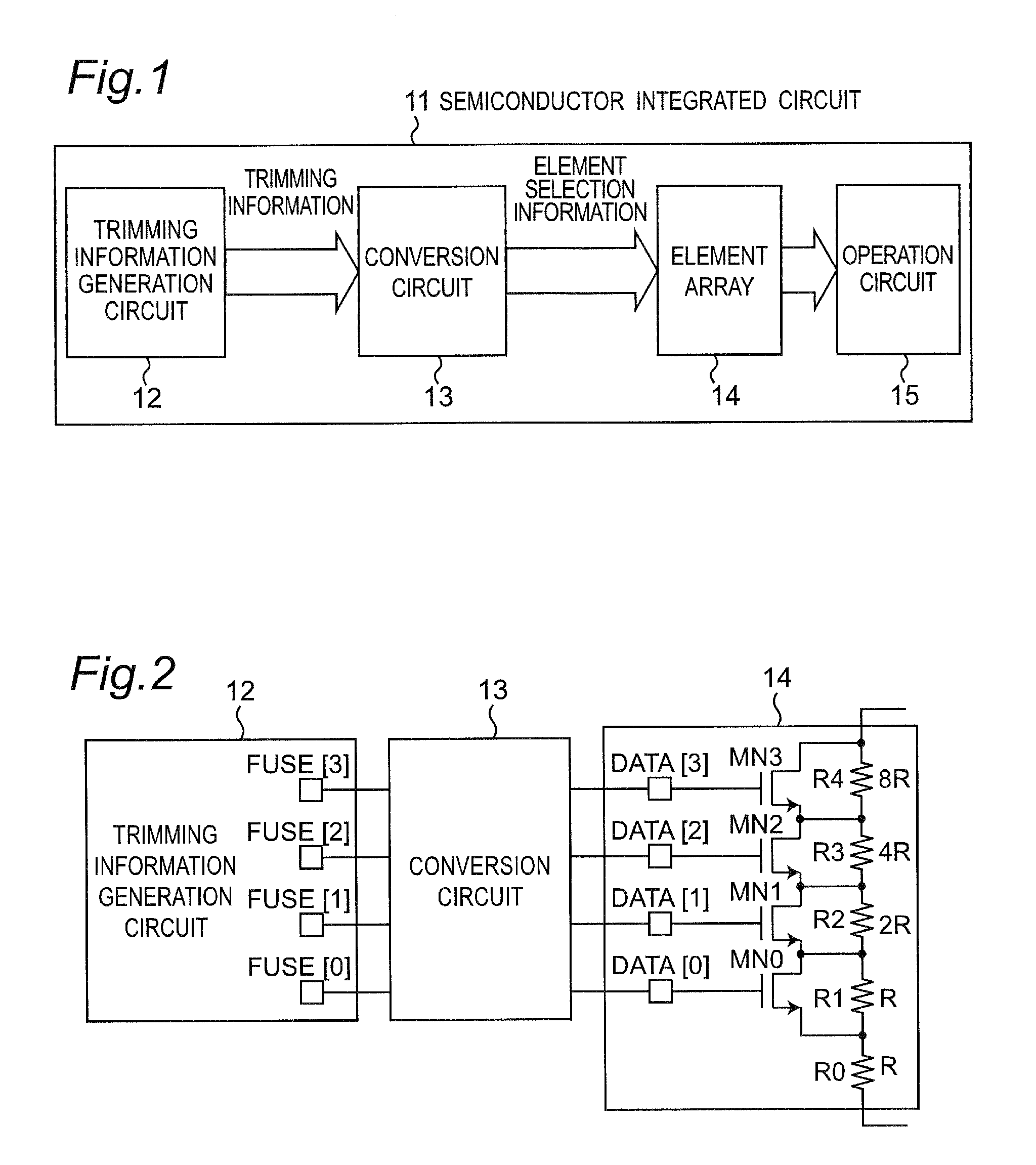
[0091]In FIG. 1, reference sign 11 denotes a semiconductor integrated circuit, which includes a trimming information generation circuit 12, a conversion circuit 13, an element array 14, and an operation circuit 15.

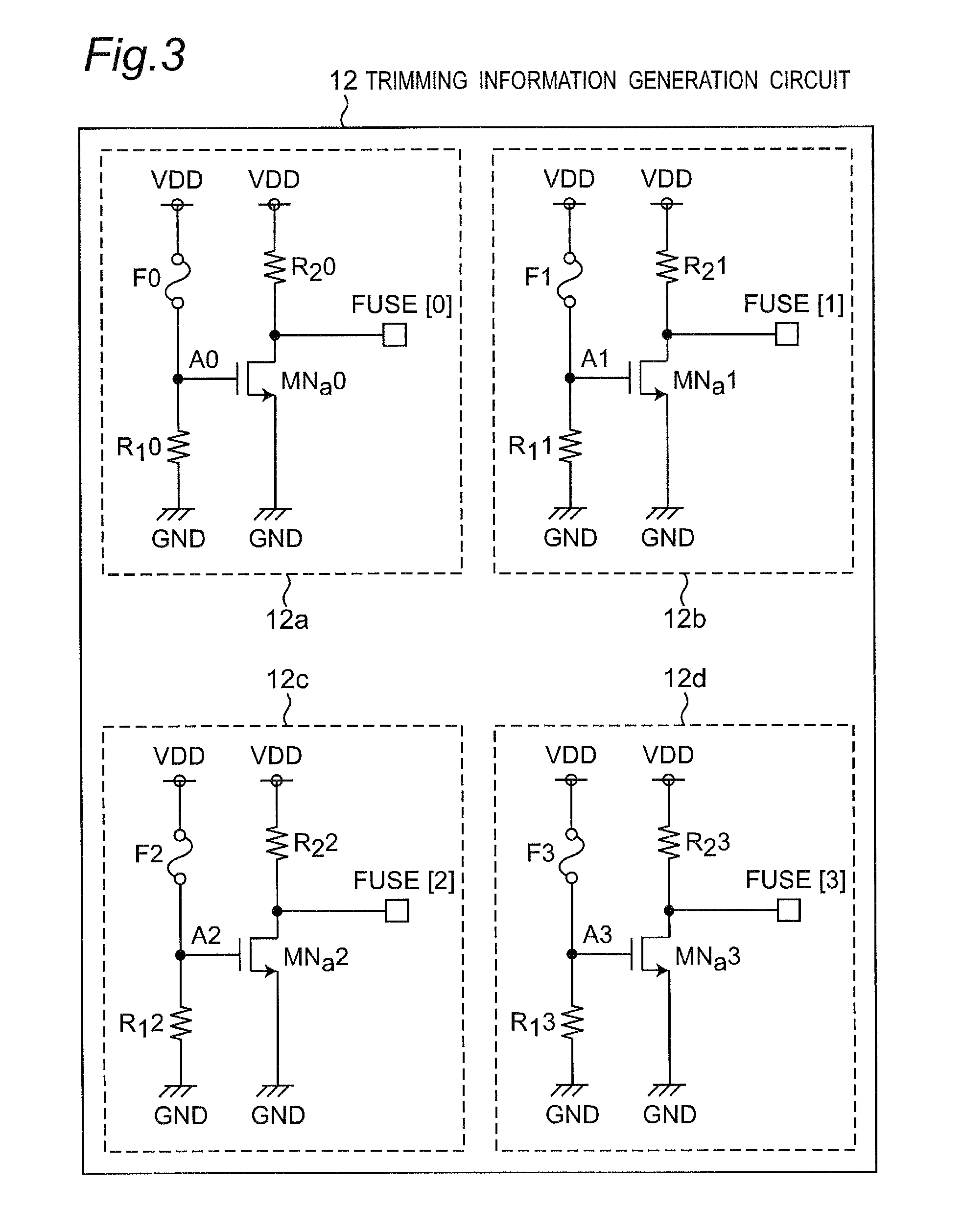
[0092]In this configuration, the trimming information generation circuit 12, having a plurality of fuses contained therein as will be detailed later, generates trimming signals representing whether or not the individual fuses have been melted and cut by trimming, and outputs trimming information formed of a bit string representing trimming signals for all the fuses.

[0093]The conversion circuit 13 performs conversion, as will be detailed later, of a bit string of trimming information outputted from the trimming information generation circuit 12 to generate element selection information formed of a bit string. According to the element selection information generated b...

second embodiment

[0138]In the first embodiment, as described above, correspondence between the combined resistance values of resistors R shown in FIG. 5C and the trimming information shown in FIG. 5A is fulfilled by setting the array of trimming information corresponding to the combined resistance values ‘16R’ to ‘9R’ into a descending order from ‘15’ to ‘8’ in decimal number. Meanwhile, the array of trimming information corresponding to the combined resistance values ‘8R’ to ‘1R’ is set into an ascending order from ‘0’ to ‘7’ in decimal number.

[0139]In this case, as can be seen from FIG. 5D, the number of melted-and-cut fuses does not simply increase in response to increases in deviation from ‘0’ fuses corresponding to the mean value in the appearance frequency distribution shown in FIG. 5E. The number of melted-and-cut fuses once decreases as from ‘3’ to ‘2’ fuses in the minus side of deviation and as from ‘2’ to ‘1’ fuses in the plus side of deviation.

[0140]From a viewpoint of lessening the numbe...


PUM


Abstract

A resistor array is provided in an element array. A mean value of a characteristic-value distribution is associated with a median of combined resistance values obtained by the element array. An array of trimming information pieces corresponding to combined resistance values larger than the median is set in a descending order of ‘15’ to ‘8’ in decimal number, and an array of trimming information pieces corresponding to combined resistance values less than the median is set in an ascending order of ‘0’ to ‘7’ in decimal number. A circuit converts trimming information derived from the trimming information generation circuit to generate element selection information for selecting turn-off resistors to obtain combined resistance values from the resistor array. Thus, the number of melted-and-cut fuses involved in generation of trimming information associated within the range of “mean value±2σ” in the distribution is reduced.

Description

CROSS-REFERENCE TO RELATED APPLICATIONS[0001]This nonprovisional application claims priority under 35 U.S.C. §119(a) on Patent Application No. 2011-256566 filed in Japan on Nov. 24, 2011, the entire contents of which are hereby incorporated by reference.TECHNICAL FIELD[0002]The present invention relates to a semiconductor integrated circuit and an optical sensor device using the semiconductor integrated circuit.BACKGROUND ART[0003]Optical sensors to be contained in portable equipment have been under desires for higher sensitivity and higher accuracy.[0004]In manufacture of such optical sensors, variations in light-reception sensitivity or characteristic variations in light-emission intensity have been at issue. As a result, there is a need for providing the semiconductor integrated circuit forming an optical sensor with a fuse-containing trimming circuit and adjusting the semiconductor integrated circuit by melt-and-cut of fuses so as to reduce the manufacturing variations of the op...

Claims


Application Information

Patent Timeline
Patent Type & Authority Patents(United States)
IPC IPC(8): H01L31/00G01J1/44G11C17/16G11C17/18H01H37/76
CPCH01H37/761G01J1/44G11C17/16G11C17/18
Inventor NODA, KAZUOINOUE, TAKAHIRO
Owner SHARP KK
Why Eureka
Try Eureka