
Static-electrical-field-enhanced semiconductor-based devices and methods of enhancing semiconductor-based device performance

a technology of static electric field and semiconductor, applied in the direction of solid-state devices, coatings, chemical vapor deposition coatings, etc., can solve the problems of low carrier mobilities, low doping efficiency, and low carrier mobility, so as to improve carrier mobility. the effect of mobility

Inactive Publication Date: 2015-04-14
VERSATILIS
View PDF7 Cites 0 Cited by
  • Summary
  • Abstract
  • Description
  • Claims
  • Application Information

AI Technical Summary

Benefits of technology

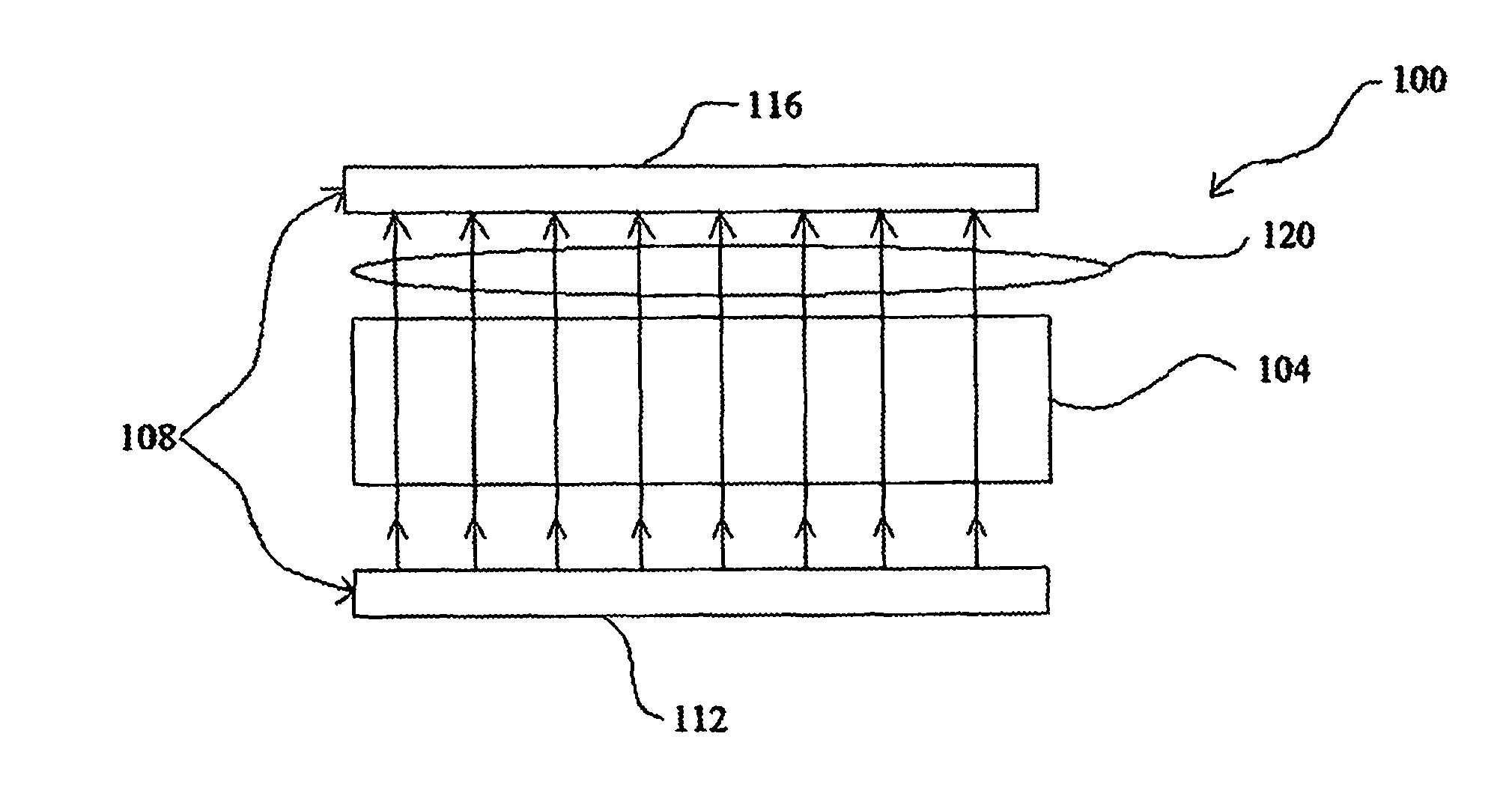
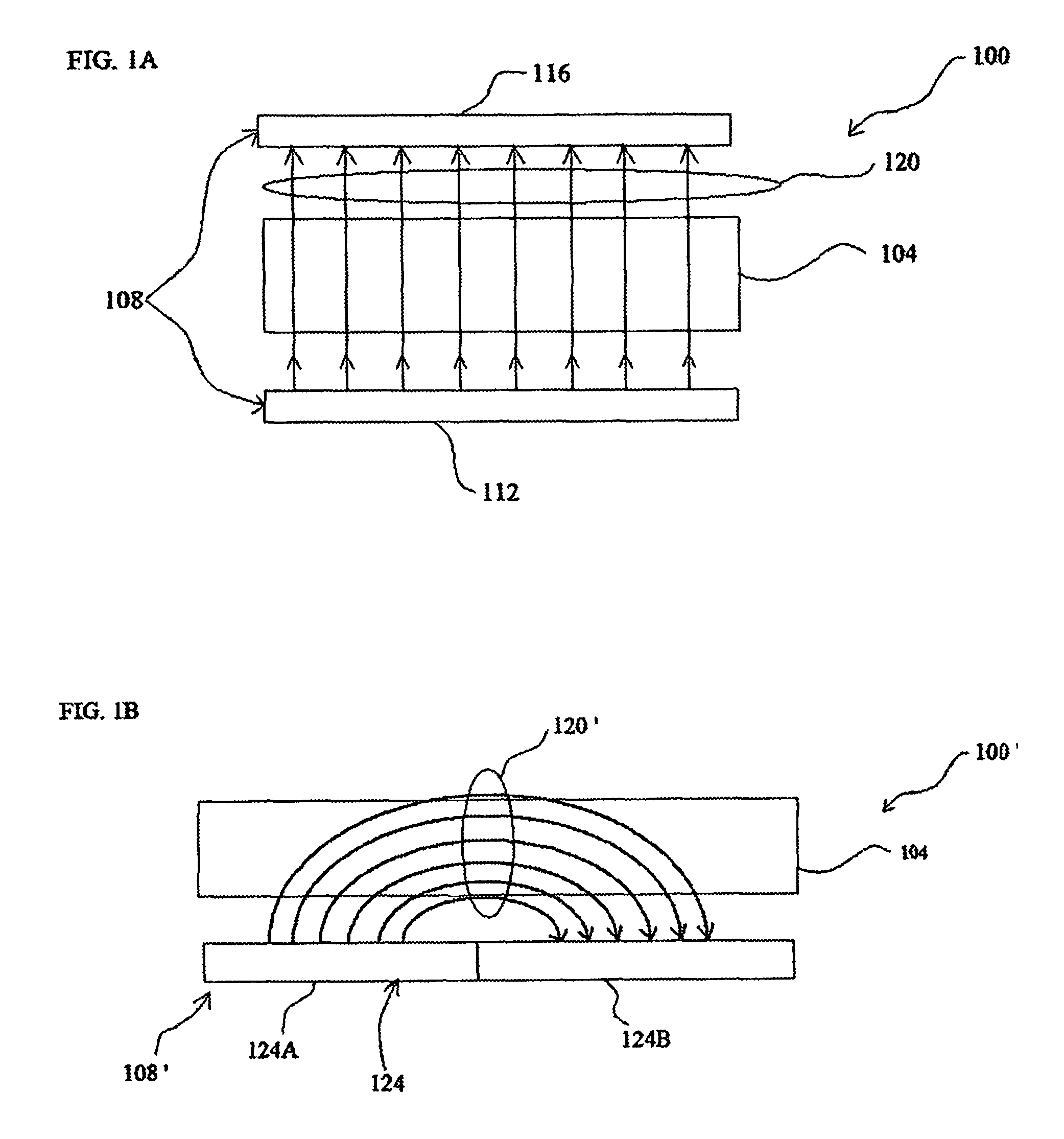
[0007]In one implementation, the present disclosure is directed to a device, including a functional semiconductor element providing, during use, at least one of 1) an electrical function and 2) an optoelectrical function; and an electric field source that produces a static electric field and includes at least one electret, the static-field source designed, configured and located in fixed relation relative to the functional semiconductor element so that the static electric field enhances carrier mobility within the functional semiconductor element.
[0010]In yet another implementation, the present disclosure is directed to a method of enhancing performance of a functional semiconductor element. The method includes providing the functional semiconductor element; and locating an electret-based electric field source proximate the functional semiconductor element so as to immerse the functional semiconductor element in a static electric field from the electret-based electric field source so as to enhance performance of the functional semiconductor element.

Problems solved by technology

However, low temperature deposition of inorganic semiconductors used in industry typically yields amorphous and polycrystalline phases of the semiconductor, and these phases tend to have significantly lower carrier mobilities than can be realized in single-crystal variants of the same semiconductor.
However, this is still significantly below single crystal silicon mobilities of >450 cm2 / Vs.
However, lower doping reduces the open-circuit voltage, Voc, of the solar cell.
However, a smaller depletion region will increase unwanted surface recombination thus the series resistance will increase.
Consequently, the solar cell's efficiency is reduced.
This means the solar cell efficiency is limited by the device and design parameters.

Method used


Image

  • Static-electrical-field-enhanced semiconductor-based devices and methods of enhancing semiconductor-based device performance
  • Static-electrical-field-enhanced semiconductor-based devices and methods of enhancing semiconductor-based device performance
  • Static-electrical-field-enhanced semiconductor-based devices and methods of enhancing semiconductor-based device performance

Examples


examples

[0075]Following are a few select examples of semiconductor-based devices that include electret-based E-field sources for “immersing” the one or more functional semiconductor elements of those devices in a static E-field so as to enhance the functioning of such element(s). These examples should in no way be taken as limiting, but rather illustrative. Those skilled in the art will readily understand how to configure other static-E-field enhanced devices using the teachings of the present disclosure.

Solar Cell Devices

[0076]FIG. 10 illustrates a solar cell device 1000 made in accordance with the present disclosure. Solar cell device 1000 includes a solar cell 1004 and an electret-based E-field source 1008 that sandwiches the solar cell between two plates 1012, 1016 of the E-field source. Solar cell 1004 can, for example, have a construction the same as or similar to the construction of virtually any solar cell based on organic and / or inorganic semiconductors. The semiconductor material ...


PUM

PropertyMeasurementUnit
band gapsaaaaaaaaaa
band gapsaaaaaaaaaa
diffusion lengthsaaaaaaaaaa

Abstract

Devices that include one or more functional semiconductor elements that are immersed in static electric fields (E-fields). In one embodiment, one or more electrets are placed proximate the one or more organic, inorganic, or hybrid semiconductor elements so that the static charge(s) of the electret(s) participate in creating the static E-field(s) that influences the semiconductor element(s). An externally applied electric field can be used, for example, to enhance charge-carrier mobility in the semiconductor element and / or to vary the width of the depletion region in the semiconductor material.

Description

RELATED APPLICATION DATA[0001]This application claims the benefit of priority of the following U.S. Provisional Patent Applications, each of which is incorporated by reference herein in its entirety: U.S. Provisional Application Ser. No. 61 / 283,265, filed on Dec. 2, 2009; U.S. Provisional Application Ser. No. 61 / 283,356, filed on Dec. 3, 2009; U.S. Provisional Application Ser. No. 61 / 343,932, filed on May 6, 2010; U.S. Provisional Application Ser. No. 61 / 343,931, filed on May 6, 2010; U.S. Provisional Application Ser. No. 61 / 396,020, filed on May 21, 2010; and U.S. Provisional Application Ser. No. 61 / 396,022, filed on May 21, 2010.FIELD OF THE INVENTION[0002]The present invention generally relates to the field of semiconductor-based devices. In particular, the present invention is directed to static-electrical-field-enhanced semiconductor-based devices and methods of enhancing semiconductor-based device performance.BACKGROUND[0003]Trends in semiconductor-based electronics industries...

Claims


Application Information

Patent Timeline
Patent Type & Authority Patents(United States)
IPC IPC(8): C23C16/44H01L31/0216H01L31/06H01L51/42
CPCH01L31/02167H01L31/06H01L51/42Y02E10/549H10K30/50H10K30/00
Inventor JAIN, AJAYKUMAR R.
Owner VERSATILIS
Learn More