Oxide sintered compact and sputtering target

a technology of sputtering target and compact, which is applied in the direction of diaphragms, conductive materials, wood working apparatuses, etc., can solve the problems of high material cost in the mass production process, and achieve the effect of low resistivity, high relative density and reduced material cos

Active Publication Date: 2015-06-16
KOBELCO RES INST
View PDF39 Cites 1 Cited by
  • Summary
  • Abstract
  • Description
  • Claims
  • Application Information

AI Technical Summary

Benefits of technology

[0022]The present invention can give oxide sintered compacts and sputtering targets each having a low resistivity and a high relative density even employing rare-metal In in a smaller amount and can thereby significantly reduce the material cost. In addition, the present invention can give sputtering targets which exhibit superior direct-current discharge stability and have excellent in-plane uniformity and satisfactory stability in film quality. The sputtering targets of the present invention, when used, enable inexpensive and stable deposition of oxide semiconductor films having satisfactory carrier mobility through direct-current sputtering, because such direct-current sputtering easily enables high-speed film deposition and leads to better productivity.

Problems solved by technology

These oxide semiconductors, however, employ indium, which is a rare metal, and may cause higher material cost in mass production process.

Method used


Image

  • Oxide sintered compact and sputtering target
  • Oxide sintered compact and sputtering target
  • Oxide sintered compact and sputtering target

Examples


experimental example 1

[0078]A zinc oxide powder (JIS Class 1, 99.99% purity), a 99.99%-purity tin oxide powder, and a 99.99%-purity indium oxide powder were blended in a ratio of [Zn];[Sn];[In] of 40.0:40.0:20.0 and mixed in a nylon ball mill for 20 hours. Next, a powder mixture obtained in the step was dried, granulated, preformed through die press at a pressure of 0.5 tonf / cm2, and compacted through CIP at a pressure of 3 tonf / cm2.

[0079]The resulting compact was sintered by holding at 1500° C. at atmospheric pressure for 7 hours. The sintering was performed in an oxygen atmosphere by feeding oxygen gas into a sintering furnace. The compact after sintering was introduced into a heat treatment furnace and heat-treated at 1200° C. for 10 hours. The heat treatment was performed in a reducing atmosphere by feeding nitrogen gas into the heat treatment furnace.

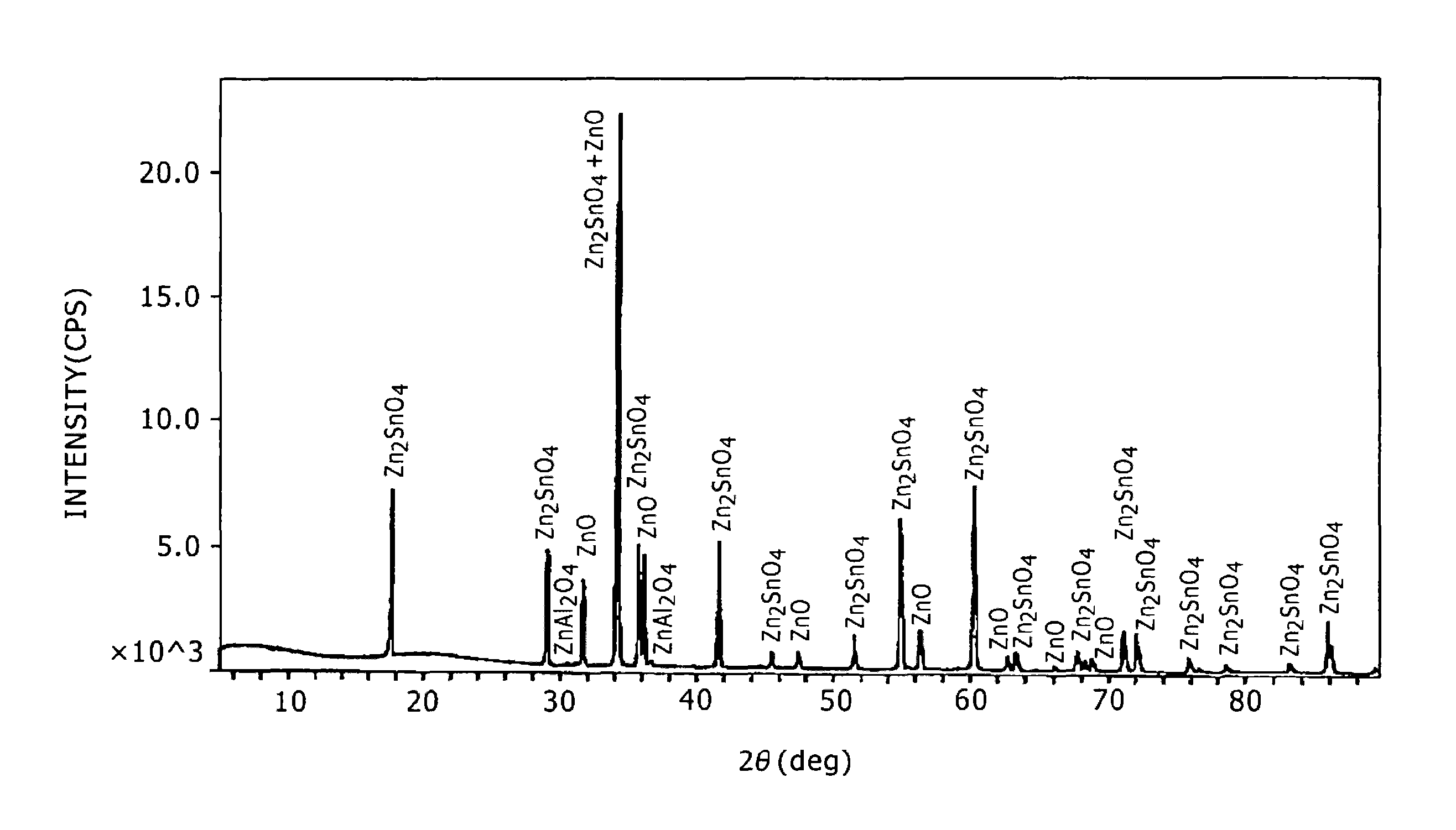
[0080]Thus, an oxide sintered compact of Experimental Example 1 was obtained. The oxide sintered compact was analyzed by X-ray diffractometry under the...

experimental example 2

[0085]An oxide sintered compact of Experimental Example 2 was prepared by the procedure of Experimental Example 1, except for blending the materials in a ratio of [Zn]:[Sn]:[In] of 48.0:32.0:20.0, sintering the compact by holding at 1550° C. for 5 hours, and subsequently subjecting the compact to a heat treatment at 1150° C. for 14 hours.

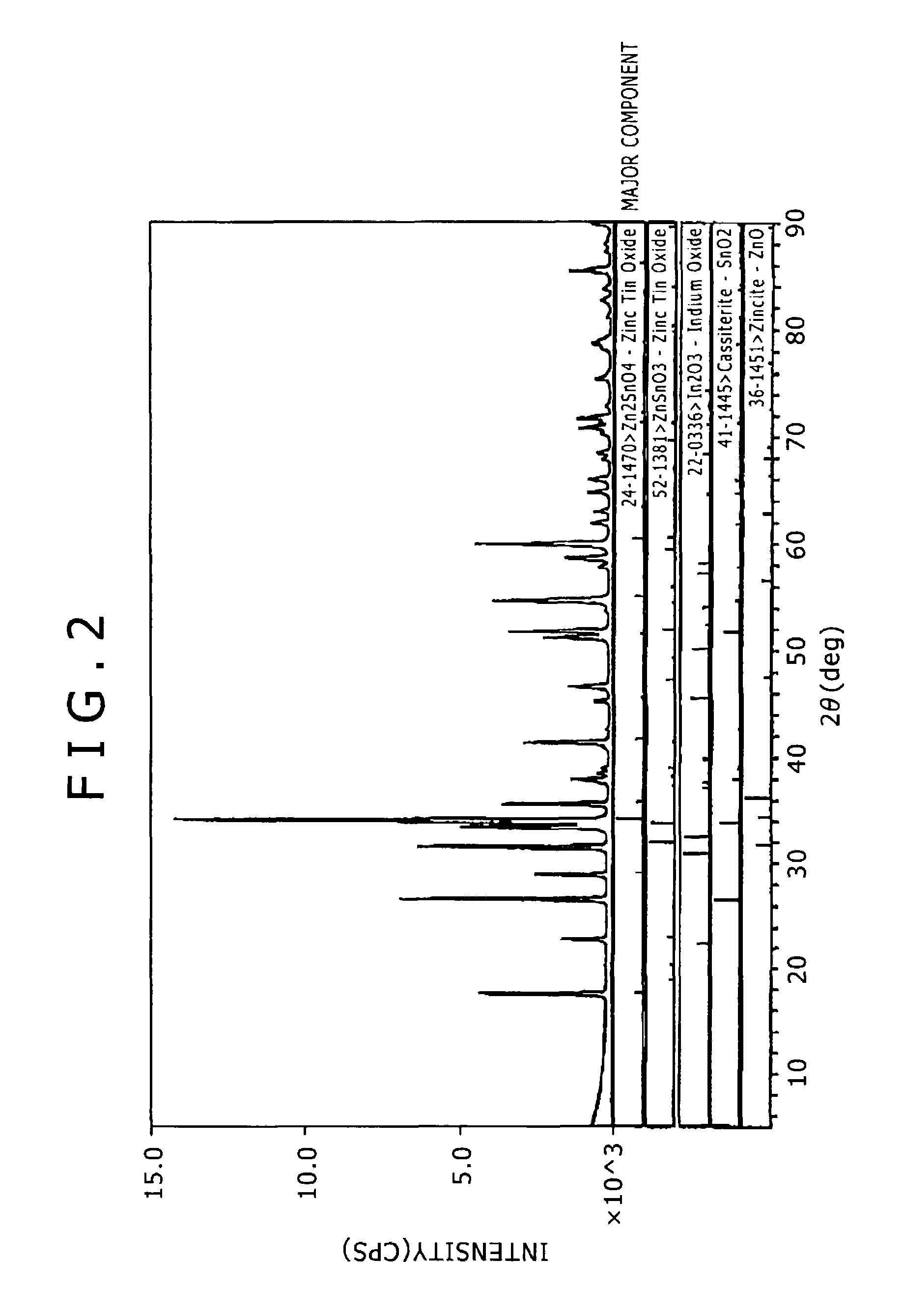
[0086]The results are indicated in FIG. 3 and as Sample No. 3 in Table 1. FIG. 3 and Table 1 demonstrate that the oxide sintered compact included Zn2SnO4, ZnSnO3, and In / In2O3—ZnSnO3 solid solution, but substantially no ZnxInyOz was detected. The oxide sintered compact was subjected to X-ray diffractometry under the conditions and was found to have a maximum peak intensity of I1 in a (311) plane of the Zn2SnO4 phase and a maximum peak intensity of I2 in a (104) plane of the In2O3 phase and to have an intensity ratio (I2 / I1) of 0.24 within the preferred range (0.5 or less) in the present invention.

[0087]In addition, the sintered compact was machined ...

experimental example 3

[0088]An oxide sintered compact of Experimental Example 3 was prepared by the procedure of Experimental Example 1, except for blending the materials in a ratio of [Zn]:[Sn]:[In] of 53.0:27.0:20.0, sintering the compact by holding at 1600° C. for 8 hours, and subsequently subjecting the compact to a heat treatment at 1200° C. for 16 hours.

[0089]The results are indicated in FIG. 4 and as Sample No. 4 in Table 1. FIG. 4 and Table 1 demonstrate that the oxide sintered compact included Zn2SnO4, ZnSnO3, and In / In2O3—ZnSnO3 solid solution, but substantially no ZnxInyOz was detected. Independently, the oxide sintered compact was subjected to X-ray diffractometry under the conditions and was found to have a maximum peak intensity of I1 in a (311) plane of the Zn2SnO4 phase and a maximum peak intensity of I2 in a (104) plane of the In2O3 phase and to have an intensity ratio (I2 / I1) of 0.15 within the preferred range (0.5 or less) in the present invention.

[0090]In addition, the sintered compac...


PUM

PropertyMeasurementUnit
electrical resistivityaaaaaaaaaa
temperatureaaaaaaaaaa

Abstract

This oxide sintered compact is obtained by mixing and sintering powders of zinc oxide, tin oxide and indium oxide. As determined by X-ray diffractometry of this oxide sintered compact, the oxide sintered compact has a Zn2SnO4 phase as the main phase and contains an In / In2O3—ZnSnO3 solid solution wherein In and / or In2O3 is solid-solved in ZnSnO3, but a ZnxInyOz phase (wherein x, y and z each represents an arbitrary positive integer) is not detected. Consequently, the present invention was able to provide an oxide sintered compact which is suitable for use in the production of an oxide semiconductor film for display devices and has both high electrical conductivity and high relative density. The oxide sintered compact is capable of forming an oxide semiconductor film that has high carrier mobility.

Description

TECHNICAL FIELD[0001]The present invention relates to oxide sintered compacts and sputtering targets for use in sputtering deposition of oxide semiconductor thin films of thin-film transistors (TFTs), which thin-film transistors are used in display devices such as liquid crystal displays and organic electroluminescent displays.BACKGROUND ART[0002]Amorphous (noncrystalline) oxide semiconductors for use in TFTs have higher carrier mobility and larger optical band gaps and can be deposited at lower temperatures than those of general amorphous silicon (a-Si) semiconductors. For these reasons, the amorphous oxide semiconductors are expected to be applied typically to next-generation displays which should have large sizes and high resolutions and should be driven at high speed; and to resin substrates which have poor thermal stability. Deposition of such an oxide semiconductor (film) preferably employs sputtering, in which a sputtering target including the same materials as the film is su...

Claims


Application Information

Patent Timeline
Patent Type & Authority Patents(United States)
IPC IPC(8): H01B1/08C04B35/453C04B35/457C04B35/626C23C14/08C23C14/34
CPCH01B1/08C04B35/453C04B35/457C04B35/6261C04B35/62695C23C14/086C23C14/3414C04B2235/3284C04B2235/3286C04B2235/3293C04B2235/80C04B2235/6567C04B2235/6585C04B2235/77C04B35/64C23C14/34
Inventor GOTO, HIROSHIIWASAKI, YUKIEHIRA, MASAYAYONEDA, YOICHIRO
Owner KOBELCO RES INST
Why Eureka
Try Eureka