

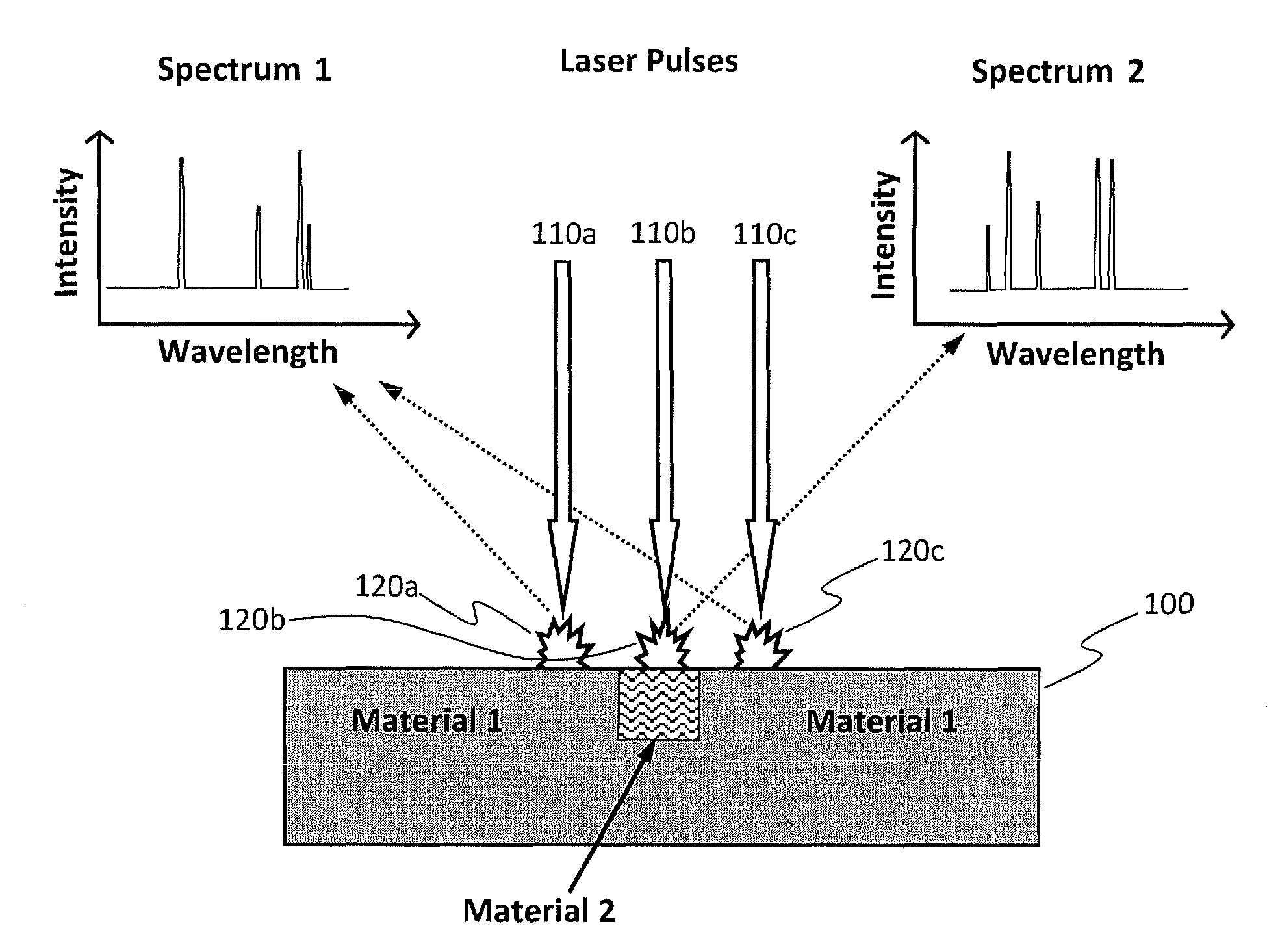
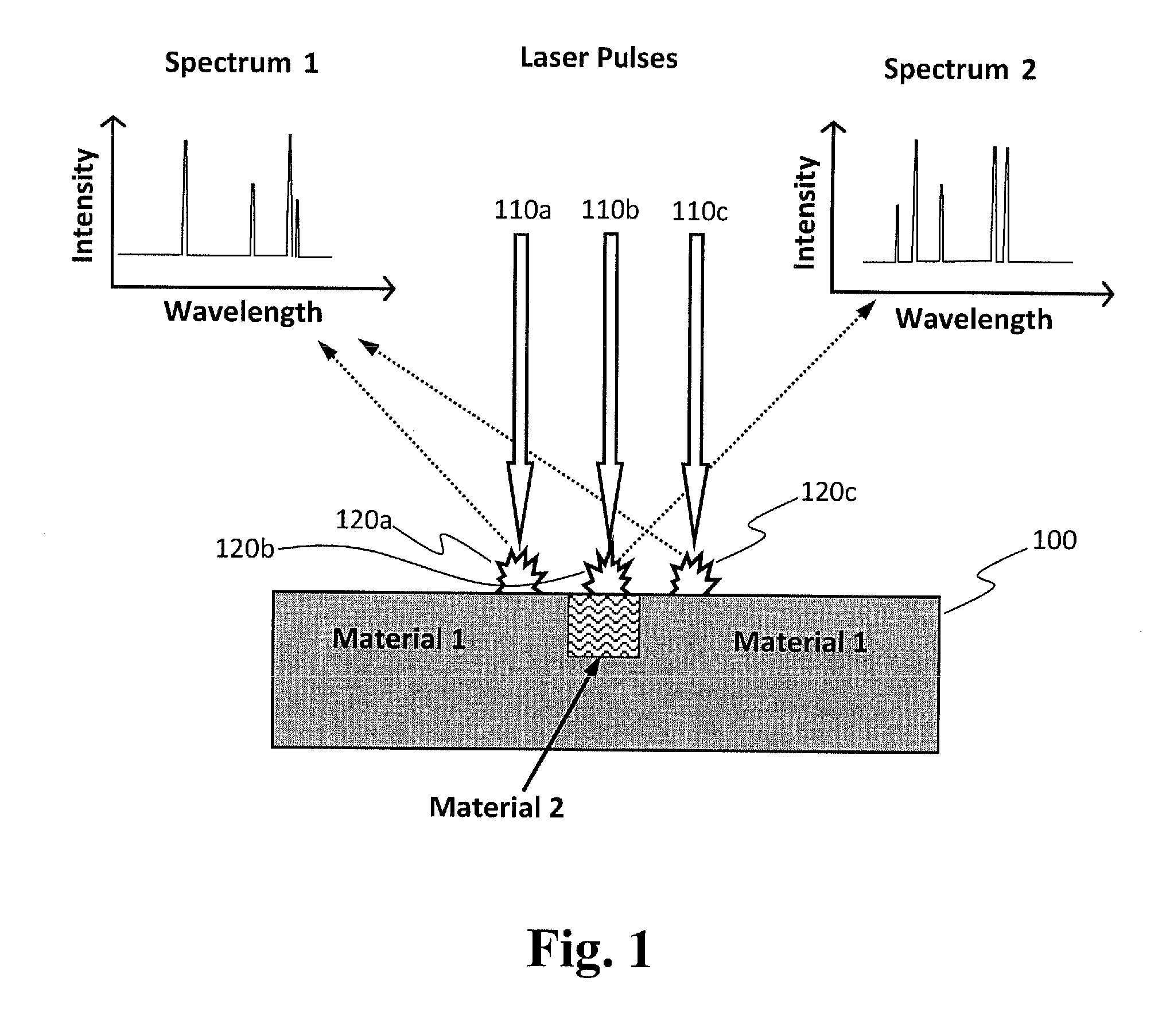
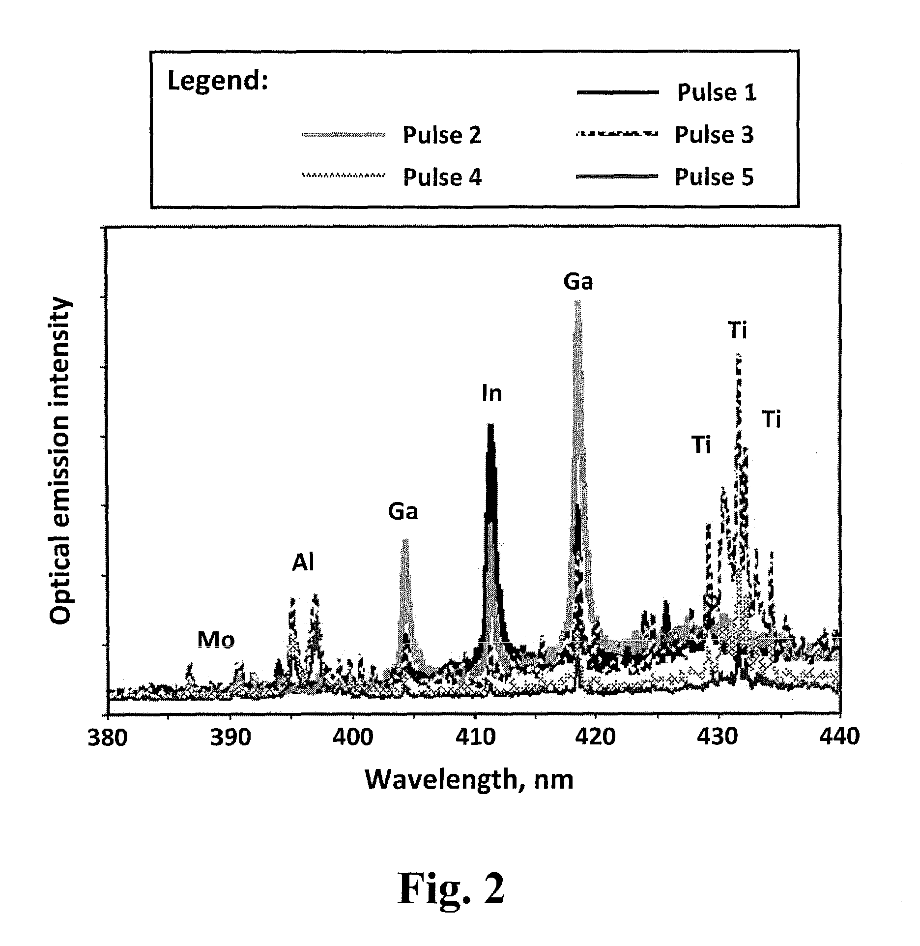
Method for real-time optical diagnostics in laser ablation and laser processing of layered and structured materials
a laser ablation and laser processing technology, applied in the direction of material analysis, instruments, manufacturing tools, etc., can solve the problems of inability to distinguish between the plastic and the underlying integrated circuit, excessive time-consuming wet etching technique, and inadvertent damage of the underlying layer of the energy laser beam, etc., to achieve excellent specificity, high efficiency and throughput, and measurement very fast
- Summary
- Abstract
- Description
- Claims
- Application Information
AI Technical Summary
Benefits of technology
Problems solved by technology
Method used
Image

Examples
Embodiment Construction
[0030]The following description is presented to enable one of ordinary skill in the art to make and use the invention and is provided in the context of a patent application and its requirements. Various modifications to the described embodiments will be readily apparent to those skilled in the art after reading this document and the generic principles herein may be applied to other embodiments. Thus, the present invention is not intended to be limited to the embodiment shown but is to be accorded the widest scope consistent with the principles and features described herein.
[0031]Various aspects of the disclosure may be described through the use of flowcharts. Often, a single instance of an aspect of the present disclosure may be shown. As is appreciated by those of ordinary skill in the art, however, the protocols, processes, and procedures described herein may be repeated continuously or as often as necessary to satisfy the needs described herein. Additionally, it is contemplated t...
PUM
| Property | Measurement | Unit |
|---|---|---|
| delay time | aaaaa | aaaaa |
| time | aaaaa | aaaaa |
| size | aaaaa | aaaaa |
Abstract
Description
Claims
Application Information