

Solid-state imaging element, solid-state imaging device, imaging apparatus, and method of manufacturing polarizing element
a technology of solid-state imaging and elements, which is applied in the direction of polarizing elements, radiofrequency control devices, instruments, etc., can solve the problems of difficult application of such a technique to an imaging device having a small pixel size, and achieve the effects of reducing the thickness of the solid-state imaging element, simple configuration and structure, and excellent extinction characteristics
- Summary
- Abstract
- Description
- Claims
- Application Information
AI Technical Summary
Benefits of technology
Problems solved by technology
Method used
Image

Examples
first embodiment
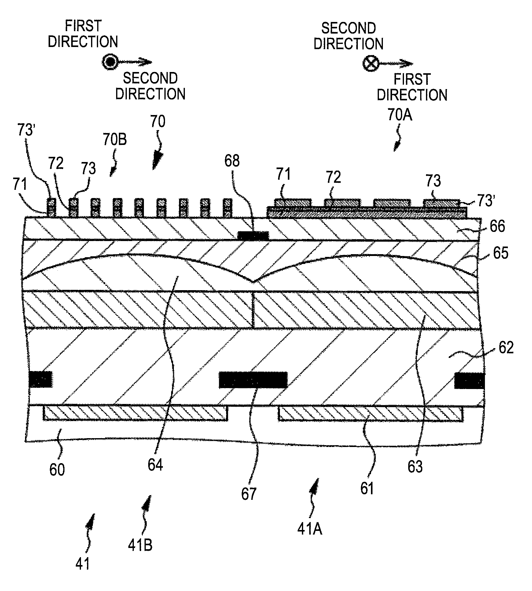
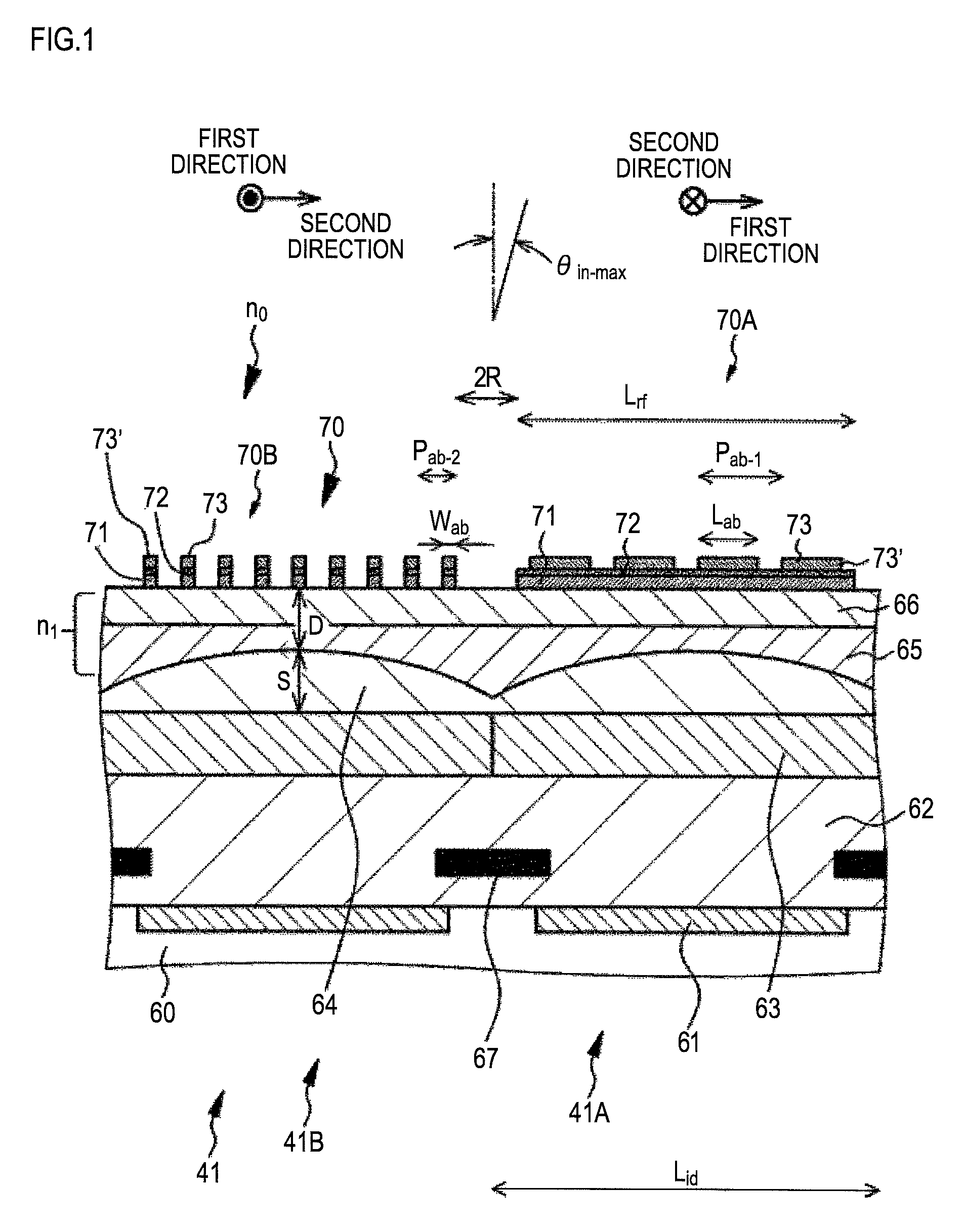
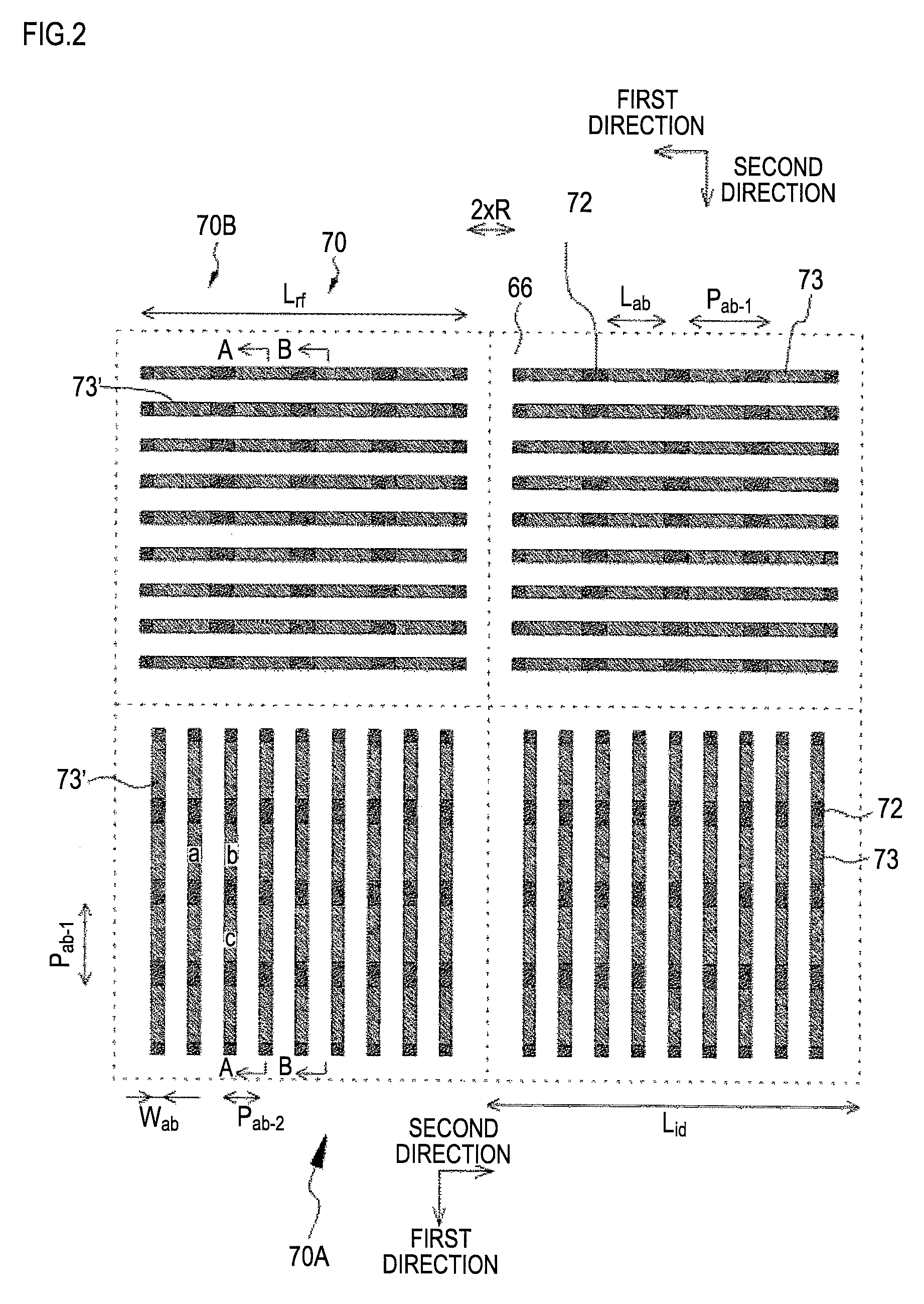
[0154]A first embodiment relates to a solid-state imaging element of the invention, a solid-state imaging device of the invention, an imaging apparatus of the present invention, and a polarizing element manufacturing method. More specifically, the first embodiment relates to the solid-state imaging element A of the present invention. A schematic partial cross-sectional view of a solid-state imaging element constituting the solid-state imaging device of the first embodiment is shown in FIG. 1, and a schematic partial plan view of the solid-state imaging element is shown in FIG. 2. A schematic partial cross-sectional view of a polarizing element is shown in (A) and (B) in FIG. 32. Two solid-state imaging elements are shown in FIG. 1, and four solid-state imaging elements are shown in FIG. 2. FIG. 1 is a schematic partial cross-sectional view taken along the arrows A-A in FIG. 2 and shows a schematic partial cross-sectional view of a solid-state imaging element along the extension dire...
second embodiment
[0191]The second embodiment is a modification of the first embodiment. The ADL method can form a film on the side surface of the polarizing element 70 more conformally than the CVD method. Thus, it is possible to prevent deterioration of optical characteristics of polarizing elements. In particular, a protective film formed of a metal oxide such as AlOx or HfOx has a high ability to protect a polarizing element and can form a film conformally in a small thickness. Therefore, such a protective film can function as a good protective film which does not deteriorate optical characteristics.
[0192]In the second embodiment, the polarizing element 70 is formed so that the formation pitch Pab-2 along the second direction is 180 nm, the width Wab is 80 nm, and the space (Pab-2-Wab) between the polarizing element 70 and the polarizing element 70 is 100 nm. Specifically, in the second embodiment, in the same step as Step-130 of the first embodiment, after removing the etching mask layer 92, a p...
third embodiment
[0194]The third embodiment is a modification of the second embodiment. In the second embodiment, the protective film 74 was also formed on the inorganic insulating base layer 66 where the polarizing element 70 is not formed. However, a further characteristic improvement (specifically, a further improvement of sensitivity) can be attained when the protective film 74 is not formed on the inorganic insulating base layer 66 where the polarizing element 70 is not formed.
[0195]In the third embodiment, in the same step as “Step-130” of the first embodiment, after removing the etching mask layer 92, a protective film 74 formed of AlOx or HfOx is formed on the polarizing element 70 (more specifically, the polarizing element 70 and the inorganic insulating base layer 66) based on the ADL method similarly to the second embodiment. Here, the protective film 74 is formed so that the thickness on the side surface of the polarizing element 70 is 15 nm (see the schematic partial cross-sectional vie...
PUM
 Abstract
Description
Claims
Application Information